


This article explores how a full bridge DC/DC converter works and how it can be used to step voltage up or down efficiently. It relies on four switching elements and a transformer to move energy between input and output while providing isolation. Such converters are widely used in power supplies, industrial electronics, and automotive systems where stable and controlled DC power is needed.
In this article we’ll explore how to implement a simple circuit for a full-bridge DC/DC converter using the Renesas HVPAK SLG47104. A complete design file is provided so readers can study the circuit and adapt the method to their own designs using Go Configure Software Hub.
Let’s dive into the implementation process. The main target parameters of the DC/DC converter:
V in = 5.0V
V out = 7.0V
I out = 0.3A
The circuit includes two functions:
- Enable with soft start
- Load current limiting
Full-bridge converter: basic theory
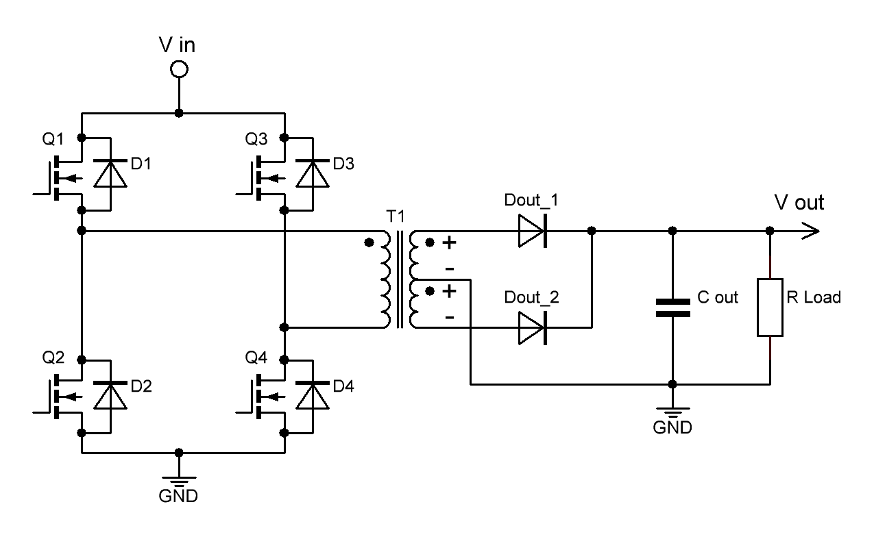
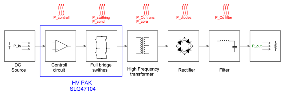
A full-bridge DC/DC converter is an electronic circuit that converts one DC voltage to another DC voltage. It utilises four switching elements (transistors) arranged in a bridge configuration and (often) a transformer to perform voltage transformation and galvanic isolation. The main circuit of the DC/DC converter is shown in Figure 1.
Operating principle
The full-bridge converter operates cyclically, with each switching period comprised of four distinct modes/states. The detailed analysis of these modes is as follows:
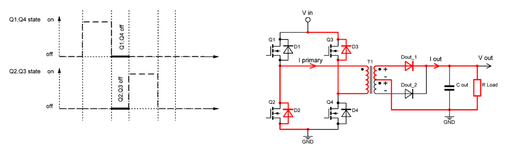
Energy transmission state
In this state, the primary side switches Q1 and Q4 are turned on, while Q2 and Q3 remain off. In this state the voltage on the second coils of the T1 transformer will have polarity shown in Figure 2. Diode Dout_1 is switched on, and the output current (I out) will increase.
Freewheeling state
In this state, the primary-side switches Q1 and Q4 are turned off. The body diodes of the switches Q2 and Q3 are turned on as shown in Figure 3, and the current that flows through the primary coil of the T1 transformer will slowly decrease. Diode Dout_1 remains switched on.
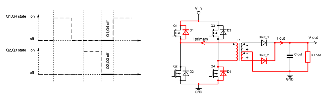
Energy transmission state
In this state, the primary-side switches Q2 and Q3 are turned on, while Q1 and Q4 remain off. In this state, the voltage on the second coil of the T1 transformer will have polarity shown in Figure 4. Diode Dout_2 is switched on, and the output current (I out) will increase.
Freewheeling state
In this state, the primary-side switches Q2 and Q3 are turned off. Figure 5 shows the body diodes of the Q1 and Q4 switches are turned on, and the current that flows through the primary coil of the T1 transformer will slowly decrease. Diode Dout_2 remains switched on.
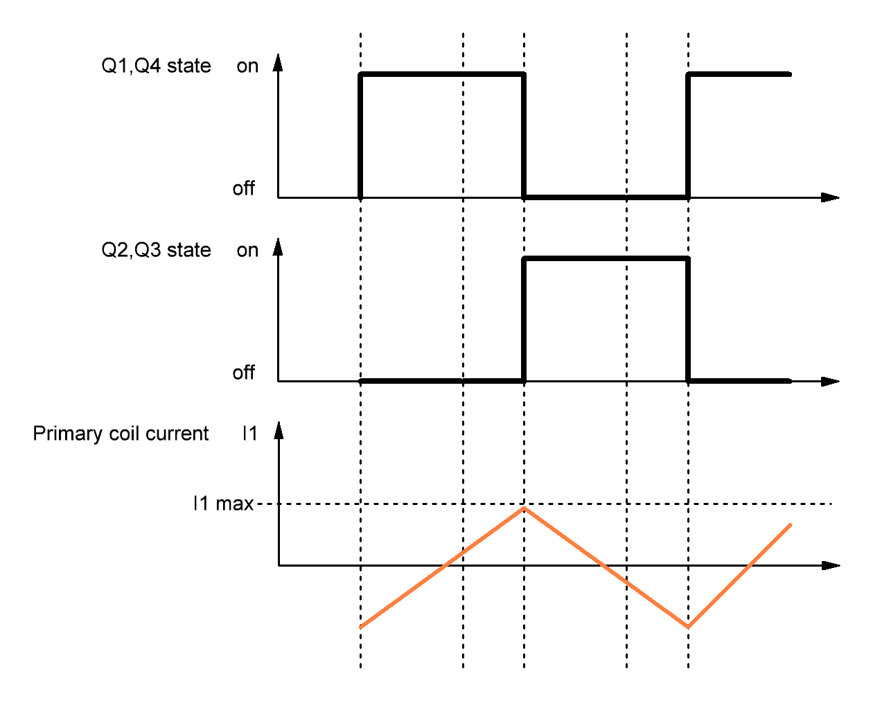
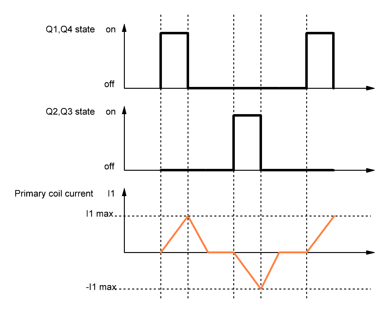
In states 1 and 3, the current through the primary winding of the transformer increases, generating a magnetic flux that induces current in the secondary winding. During states 1 and 3, if the current reaches its maximum value (I1 max), the power transistors are turned off, and the current in the primary winding reverses direction. The reverse direction current will also generate magnetic flux. This reversal occurs in states 2 and 4 due to the body diodes of the power transistors.
Figure 6 shows the primary current not able to reach the I1 max current, while Figure 7 shows the timing diagram when the primary current reaches the I1 max current.
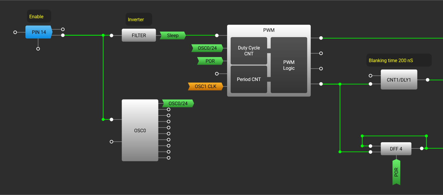
GreenPAK design
The GreenPAK Design for the Full-bridge Transformer Driver is shown in Figure 8.
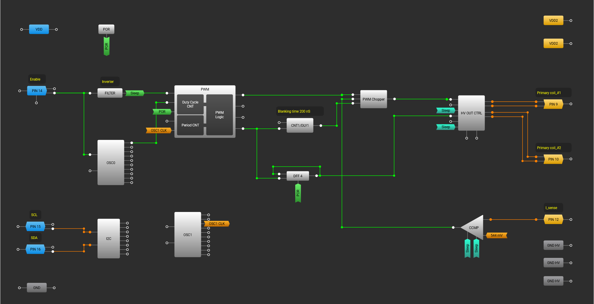
The main components of the full-bridge DC/DC converter consist of the PWM, the PWM Chopper, and the HV OUT CTRL blocks.
The PWM block generates a ~200kHz signal with soft-start, ramping the duty cycle from 0% to 100%. The full bridge DC/DC frequency is not equal to the PWM block frequency; this frequency is half of the PWM frequency – ~100 kHz.
The soft-start duration is approximately 1 second and is provided by the OSC0 block with a divider of 12 (OSC0/12). The PWM block is also used to generate pulses for switching between State 1 and State 3. For generating these pulses, DFF 4 is used. The DFF 4 output switches between HIGH and LOW every PWM period (Figure 9).
PIN 14 provides an Enable signal for the entire circuit. The enable level for the PWM block is LOW, so an inverter is used on the FILTER macrocell. The OSC0/24 clock is connected to the duty cycle control input of the PWM block (Figure 9) providing the soft-start functionality mentioned previously.
The main function of the PWM Chopper is to reduce the primary current at the switching primary coil. The blanking time for the PWM Chopper is 200 ns, which is defined by CNT1/DLY1 (see Figure 10).
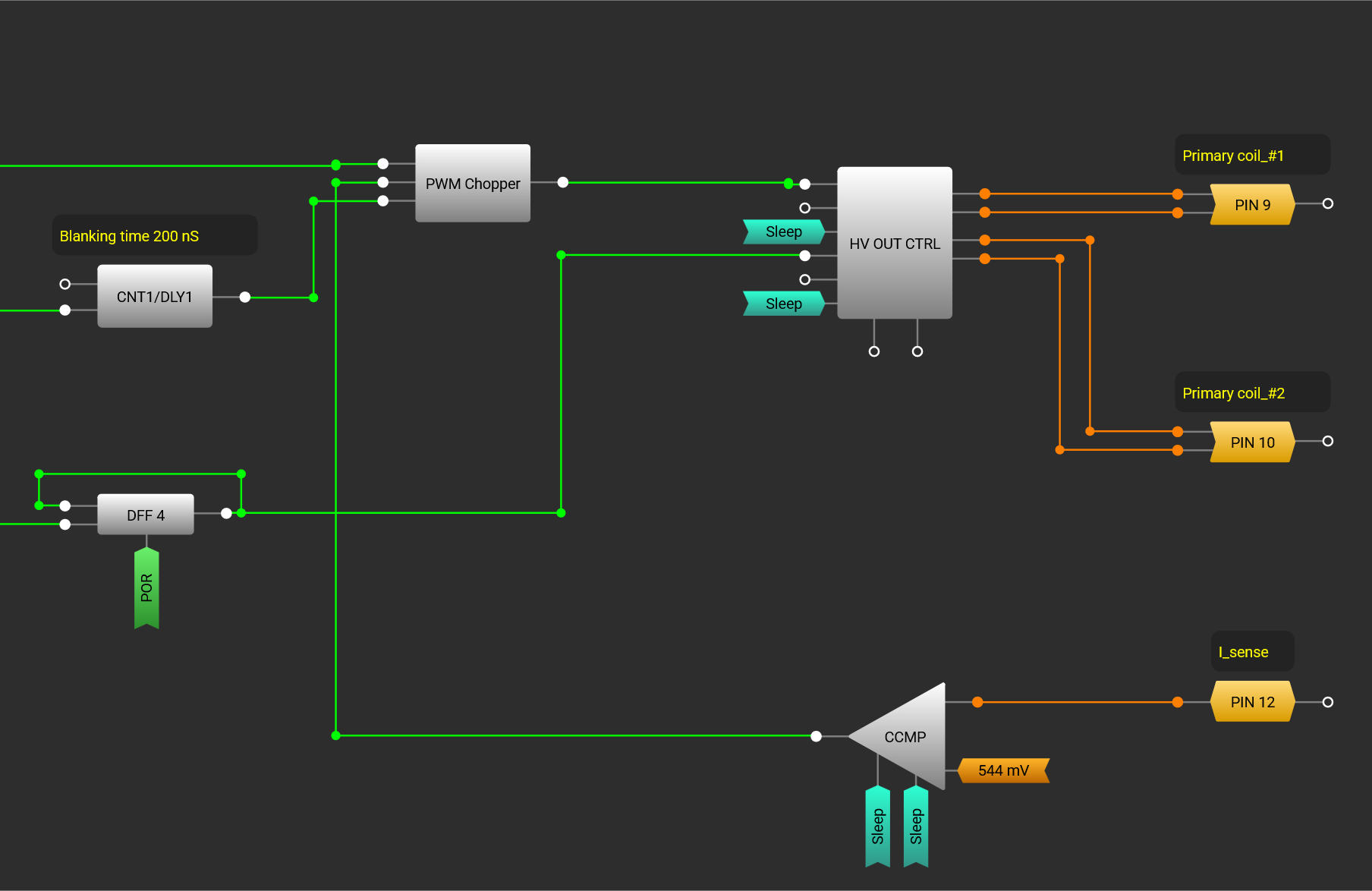
When the primary coil starts switching (state 1 or 3), during the first 200 ns blanking time, the PWM Chopper will ignore the state of the CCMP and the PWM Chopper output will be HIGH. When the current reaches the trim value, the PWM Chopper output will switch to a LOW state until the next period of the PWM module.
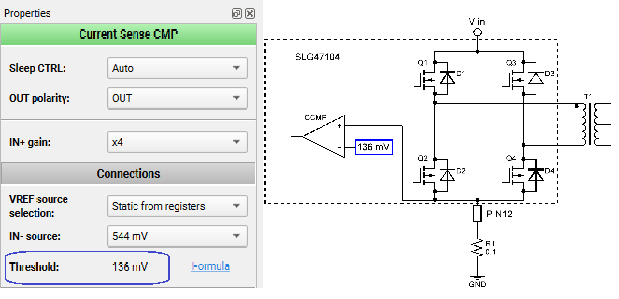
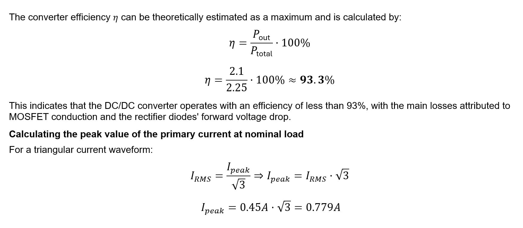
To limit the output power, the maximum primary current (Iprim max, peak value) is set to 1.36A, which corresponds to a CCMP threshold of 0.136mV with a Rsense of 0.1 Ω and is set by the CCMP (see Figure 11). Pin 12 is connected to the sources of the power MOSFETs, so this pin must be connected to GND across the current sense resistor (R1). Calculation of the peak value of the primary current and selection of the CCMP threshold value are shown in Calculating the Peak Value of the Primary Current at Nominal Load section.
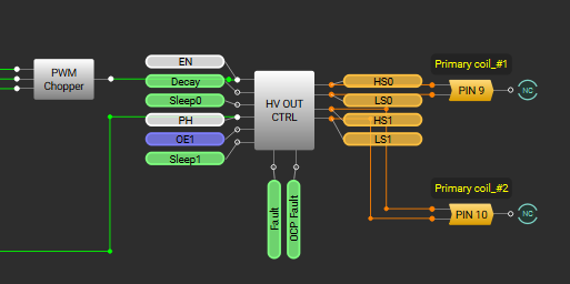
The HV OUT CTRL block is configured as a PH-EN (phase-enable) full-bridge. The logic level at the PH input determines the polarity of the voltage applied to the primary coil. The output of DFF 4 changes the logic level at PH every PWM period, resulting in the HV output switching (changing the polarity at the primary coil) at a frequency of 100kHz. The EN (enable) input of the HV OUT CTRL block determines how long the transformer’s primary coil remains connected to the power source (Vin). The EN input is connected to the PWM Chopper output, so the duration of the EN input’s high level is dependent on the CCMP.
The HV OUT CTRL block is shown in Figure 12.
Calculation of the high-frequency transformer
Input data for calculation transformer
- Vin = 5V
- Vout = 7V
- Iout = 0.3A
- fsw =100kHz
- Rectifier diodes SS14, Vf = 0.2V
- Transformer core – type RM6, ferromagnetic material N87
Calculating the number of turns of the primary winding
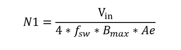
For the RM6 transformer core:
B_max = 0.18T (Maximum magnetic flux density)
Ae = 20×10⁻⁶ m² (Effective cross-sectional area)
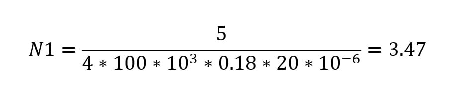
The practical significance of the number of primary turns becomes:
Calculating the number of turns of the secondary winding
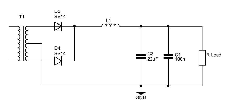
In a full-bridge DC/DC converter with a centre-tapped secondary winding, the number of turns on the secondary winding determines the output voltage. For a center-tap configuration (Figure 13), the secondary winding is split into two halves, each conducting alternately through the diodes.
The half-secondary turns can be calculated as:
where:
- N_”half” – number of turns in one half of the secondary
- N_1 – number of primary turns
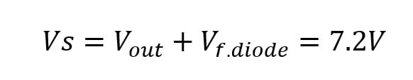
- V_”s” =V_”out” +V_f – voltage across one half of the secondary, including forward voltage drop of the diode
- V_”in” – input DC voltage to the full-bridge
To calculate the half-secondary turns
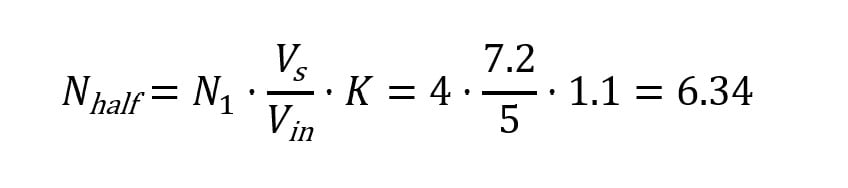
Note: *K = 1.1 – factor for compensating losses in the filter (and other losses).
The practical significance of the number of turns:

Theoretical efficiency
Input data for calculating the efficiency of a DC/DC converter
- V_in = 5V
- V_out = 7V
- I_out = 0.3A
- SLG47104, Rds_on = 0.25Ω
- Rectifier diodes SS14, Vf = 0.2V
Every DC/DC converter experiences an inherent power loss during the voltage conversion process. Figure 14 illustrates a simplified block diagram of the converter and highlights the primary points where these losses will occur.
Basic formula for calculating the efficiency (η) of a DC/DC converter:


Efficiency calculation
Based on the calculated peak current at nominal load, the primary winding current under short-circuit conditions is assumed to be 1.5A, which is twice the peak value. The nearest CCMP switching voltage for Rsense = 0.1 Ω corresponds to a threshold of 136mV.
Device testing
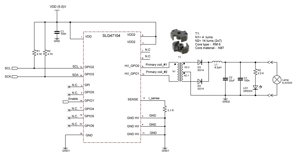
Figure 15 shows the circuit diagram of the test board, and Figure 16 shows the test board, which is used for evaluating the DC/DC converter.
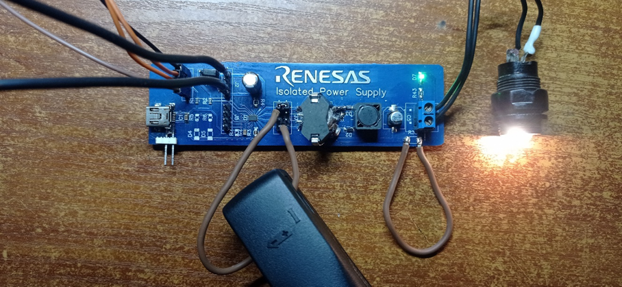
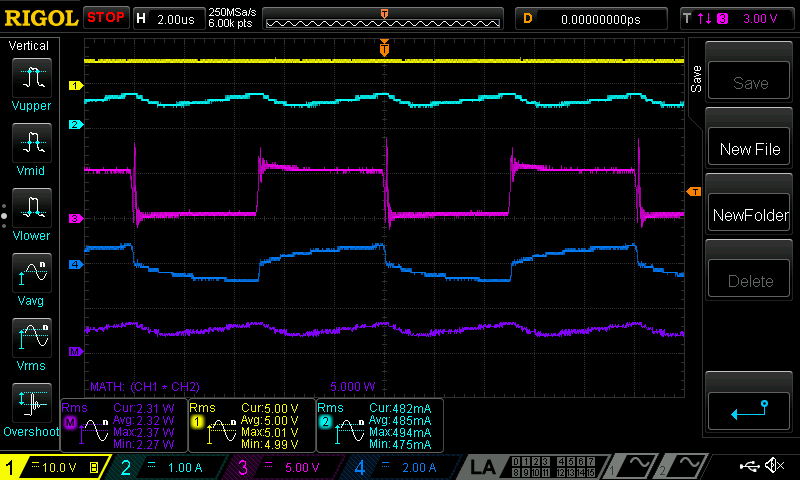
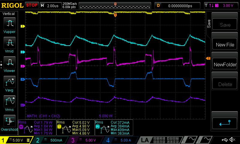
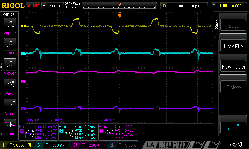
Nominal load test (lamp 6.3V, 2W connected to test board)
Channel 1 (yellow/top line) – Vin
Channel 2 (light blue/2nd line) – Iin
Channel 3 (magenta/3rd line) – PIN#9 (Primary coil_#1)
Channel 4 (blue/bottom line) – Primary coil current
Channel M (violet line) – Input Power (Total power)
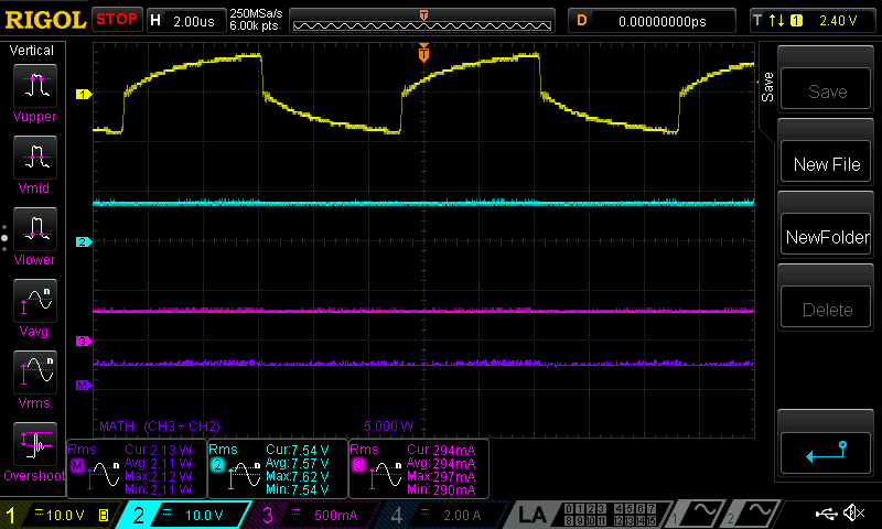
Channel 1 (yellow/top line) – Primary coil current
Channel 2 (light blue/2nd line) – Vout
Channel 3 (magenta/3rd line) – Iout
Channel M (violet line) – Output Power
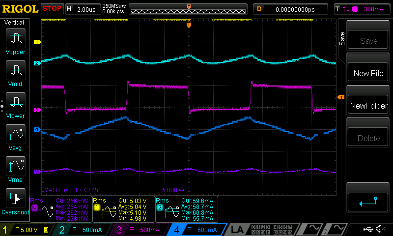
No load test (lamp disconnected, green LED connected to output)
Channel 1 (yellow/top line) – Vin
Channel 2 (light blue/2nd line) – Iin
Channel 3 (magenta/3rd line) – PIN#9 (Primary coil_#1)
Channel 4 (blue/bottom line) – Primary coil current
Channel M (violet line) – Input Power (Total power)
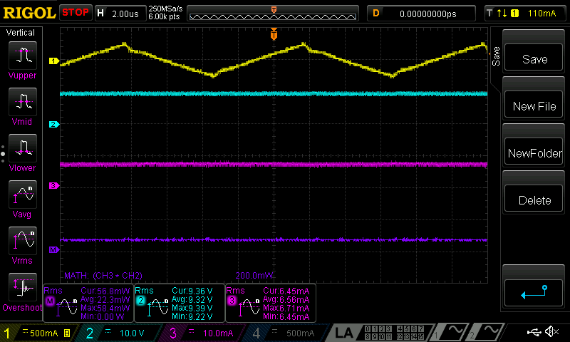
Channel 1 (yellow/top line) – Primary coil current
Channel 2 (light blue/2nd line) – Vout
Channel 3 (magenta/3rd line) – Iout
Channel M (violet line) – Output Power
Short circuit at load side
Channel 1 (yellow/top line) – Vin
Channel 2 (light blue/2nd line) – Iin
Channel 3 (magenta/3rd line) – PIN#9 (Primary coil_#1)
Channel 4 (blue/bottom line) – Primary coil current
Channel M (violet line) – Input Power (Total power)
Channel 1 (yellow/top line) – Primary coil current
Channel 2 (light blue/2nd line) – Vout
Channel 3 (magenta/3rd line) – Iout
Channel M (violet line) – Output Power
Conclusion
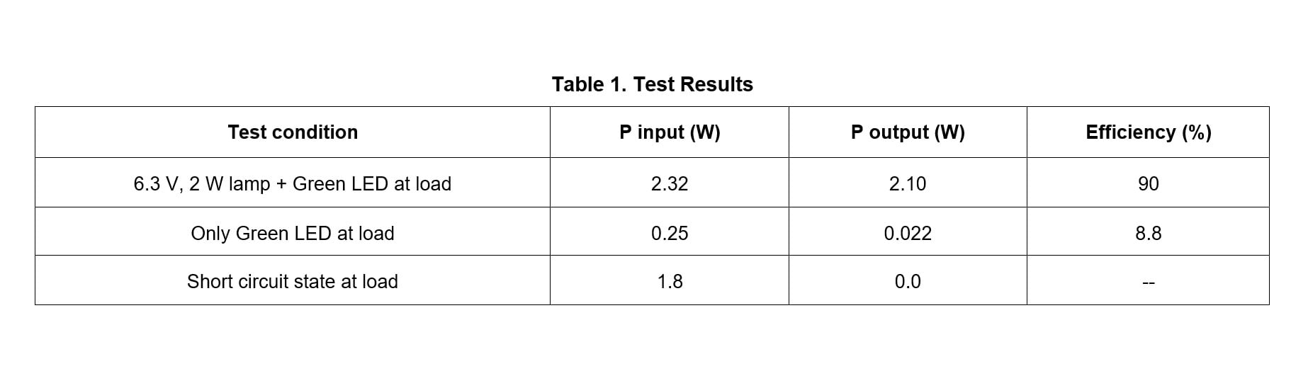
The results in Table 1 clearly demonstrate that the design reaches its highest conversion efficiency at nominal load. The drop in power consumption under short-circuit conditions verifies that the primary-side current-sense comparator operates as intended. These results demonstrate both strong efficiency at typical operating points and reliable protection behaviour.