







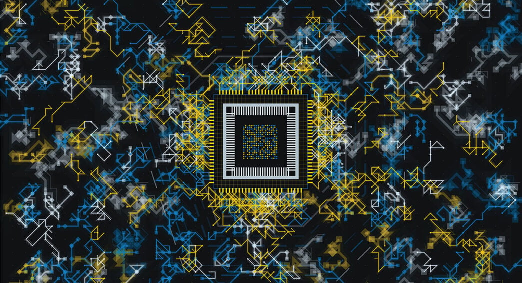
Researchers at National Yang Ming Chiao Tung University (NYCU) in Taiwan, working with TSMC Corporate Research, have discovered a way to build a smoother, higher-quality insulating layer on 2D MoS2 transistors with strong control over switching and very little wasted/leaked electricity.
For years, computer chips have improved because their switches have shrunk. This is because every chip is packed with billions of tiny transistors. The smaller the transistor, the more you can fit on a chip. The more you can fit on a chip, the faster and more efficient a product becomes.
The challenge with shrinking these switches is that they use silicon, and silicon is starting to hit a wall. The wall is that it is becoming difficult to shrink it any more without things breaking down.
But silicon has been used for years, so what material is the best to pick up the mantle?
The research team are investigating molybdenum disulphide (MoS2), a material that is only one atom thick, which is a major draw because the thinner the material, the smaller and more efficient the switches, in theory.
The traditional trade-off
To make transistors work, you need to place a very thin insulating layer on top of the material, which acts like a control, enabling the switch to be flipped on and off. This is something that has been achieved with silicon. Yet, traditional silicon fabrication methods now slow everything down, rather than speed it up. However, MoS2, being only one atom thick, is incredibly delicate. When you deposit an insulating layer on MoS2 using traditional methods, it tends to become rough and disturbs the surface. That roughness then hinders electrons as they are trying to flow through the material smoothly.
This leaves a trade-off. Either make the insulting thinner, which gives better control over the switch but damages the material underneath, affecting performance; or keep the material pristine, yet the insulating layer is not thin enough to be really useful.
How to solve a problem like boundaries
Taking a fresh approach to this challenge, the team decided against searching for a whole new material to replace MoS2. Instead, they focused on fixing the seam – the boundary where the MoS2 meets the insulating layer above it.
They achieved this by gently depositing an extremely thin layer of aluminium metal directly onto the MoS2, which was then exposed to a small amount of oxygen, turning the aluminium into aluminium oxide – a ceramic-like insulating material. This layer was incredibly thin, at around 0.42 nanometres, which is among the thinnest of its kind. This ultra-thin, smooth layer offered a clean and even foundation, on which the team could build the working insulating layer (a hafnium oxide gate dielectric) needed for the transistor to function. Owing to its smooth and even properties, the first primer layer protected the delicate MoS2 underneath from getting roughed up. Meaning electrons could keep flowing smoothly, while still getting a thin and effective insulating layer on top.
This means that, for the first time, a transistor managed to have all of the key ingredients that researchers have been searching for and that industry wants. A thin insulating layer that responds sharply and efficiently to voltage changes, very little wasted/leaked electricity when the switch is supposed to be off, and a stable, reliable operation.
Professor Wen-Hao Chang, the study’s corresponding author, said that the work shows that improving these ultra-thin transistors isn’t only about finding better semiconductor materials – the atomic interface between materials matters just as much, and engineering that boundary helped the team to reduce a trade-off that has limited 2D transistors for years.
Looking forward
The team believes that this technique is not a one-off trick only suitable for MoS2. They believe it could potentially be adapted as a general method for other similar 2D materials as well.
For the labs and companies working on these ultra-thin materials, it means that it won’t just be about who has the best raw material; it’ll be about who can engineer the connections between those materials more precisely.
This research provides the proof and reasoning behind the fact that ultra-thin 2D materials are now creeping closer to being practical for real manufacturing. And Taiwan’s chip industry is positioning itself at the centre of that research.