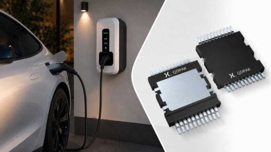


Nexperia announced the release of 1200V silicon carbide (SiC) MOSFETs in QDPAK packaging, extending its wide-bandgap (WBG) portfolio with a top-side cooled surface-mount package optimised for high-power density and thermally demanding applications.
Designed for high-efficiency, high-voltage power conversion applications, these devices enable the electrical performance of Nexperia’s SiC technology with simplified thermal management and mechanical integration, enabling higher output power, increased efficiency and improved thermal performance in compact designs.
Available in both industrial-grade and automotive-qualified variants, the portfolio offers RDS(on) options of 17, 30, 40, 60 and 80mΩ, delivering a scalable QDPAK platform for applications ranging from high-power systems to compact designs with demanding thermal and mechanical constraints. Complementing Nexperia’s existing package portfolio, QDPAK gives designers greater flexibility to optimise efficiency, power density, and thermal performance.
QDPAK packaging addresses a key limitation in high-voltage power conversion systems: heat dissipation through the PCB. By enabling a direct die-to-heatsink thermal path from the top side of the package, these devices reduce reliance on the board as the primary heat-spreading path and allow the semiconductor and PCB thermal domains to be managed more independently. Compared to conventional D2PAK-7 packaging, top-side cooled packages can deliver up to 3kW higher output power at comparable thermal limits, while also providing around 40°C additional thermal headroom at the same power level. Building on the existing X.PAK platform, QDPAK further extends power handling capability, enabling operation at approximately 3kW higher power at comparable case temperatures, while offering around 23°C additional thermal headroom at similar power levels. Well suited for EV onboard chargers (OBC), high-voltage DC-DC converters, EV charging infrastructure, photovoltaic inverters, uninterruptible power supplies (UPS), motor drives, and data centre power systems, QDPAK devices help engineers optimize both electrical and mechanical system performance.
“As wide-bandgap technologies continue to reshape power conversion design, the industry is facing a new set of thermal, mechanical and efficiency challenges as systems become smaller, denser and more power hungry,” says Gaetano Pignataro, Head of SiC & IGBT Product Group at Nexperia. “At Nexperia, we are focused on developing solutions that address these real system-level challenges. Our 1200V SiC MOSFETs in QDPAK combine the performance of our SiC technology with the thermal advantages of top-side cooling, giving engineers a practical and scalable option for next-generation high-power applications.”
Nexperia’s 1200V SiC MOSFETs in QDPAK leverage the benefits of top-side cooled surface-mount packaging with the electrical characteristics required for efficient high-voltage power conversion. Excellent RDS(on) temperature stability supports predictable conduction losses and reliable operation at elevated junction temperatures, while low-inductance package design and controlled switching behaviour support efficient operation. The additional Kelvin source pin enables faster commutation and improved switching control, helping designers manage ringing, EMI, and switching transients.