


In this article, Gordon Shen, Principal IC Architect, Synaptics Incorporated, explores the problem of EMI common in smartphones utilising OLED touchscreen and offers a solution to the challenge that has plagued OEMs since the early 2000s.
Organic light-emitting diode (OLED) displays are now commonplace, with over 60% of devices manufactured today using this technology and over 80 different smartphone models from across the biggest smartphone manufacturers integrating OLED panels in recent production cycles. However, there is a problem with OLEDs that is becoming more serious – touch to display (T2D) interference can produce visual artifacts on OLED screens.

OLEDs started being used in smartphones in the early 2000s. It has long been known that OLED touchscreens can be affected by T2D interference, but if design engineers compensated for it, issues could be mitigated. As the technology has been more widely embraced, OLED touchscreens have been developed to become thinner, resulting in them becoming significantly more susceptible to T2D interference. These issues are typically picked up during the quality control (QC) process at manufacturers, so few consumers ever experience a problem with their handset.
Beyond the environmental impact of discarding handsets with faulty displays, there are also significant costs associated with stripping down and recycling components as well as the initial manufacturing costs. As screens get thinner, the number of susceptible units being caught by QC is believed to be exceeding the Acceptable Quality Limit (AQL) for smartphone OEMs. Understandably, there are no market statistics available to evidence this, but again, the physical phenomena involved are well understood.
The need for a solution may be implicit, but it is clear.
The best solution is a new, patented approach called zero row sum code division multiplexing (CDM) driving. Zero row sum CDM is effective for any electronic system that incorporates an OLED touchscreen.
Touchscreen interference
T2D signal interference has been a challenge for on-cell OLED touchscreens since the introduction of the technology.
Display electronics and touchscreen electronics are, by necessity, close together in an OLED touchscreen. When smartphone manufacturers began to switch over to OLED screens in the early 2020s, the distance between touch drivers and the display was about 10μm. With that gap, the influence of any electromagnetic interference (EMI) from the touchscreen drivers is manageable.
Smartphone manufacturers are constantly making their devices physically lighter and more tightly integrated, and the distance between touch drivers and screen in the most advanced handsets is now commonly only 6μm, close enough that T2D interference has become a problem that requires new techniques to solve.
T2D interference can result in several impairments, including screen flicker and the appearance of patterns in what should be uniform fields. This problem is going to get worse when smartphone OEMs reduce the gap to 5μm or even 4μm, as some smartphone OEMs are attempting to do now.
Why traditional CDM falls short
The common technique used in touchscreen position detection is multidrive CDM. Touchscreens have electrodes positioned around the screen. When a user touches the screen, the position of the touch is detected by taking measurements of the horizontal electrodes and of the vertical electrodes and combining the sums.
All of the signals being in phase will result in a certain amount of T2D interference. The goal is to minimise this interference by reducing the sum of the measurements, with the sum being the difference between the number of electrodes measured in one phase and the number measured 180° out of phase.
To this end, engineers have been devising touchscreen detection schemes in which as many electrode signals as possible are 180° out of phase with one another, resulting in a low-sum CDM. The ideal would be a perfect balance, thereby achieving a zero sum, in which the signals would cancel each other out, leading to virtually no T2D interference.
Significant engineering resources have been invested in devising low-sum CDM drives. In practice, a system with 12 positive electrodes and eight negative electrodes has a sum of four. The amount of interference is reduced concomitantly. Progress was measured by lowering the sum. One subsequent example featured nine positive and seven negative electrodes, rendering a sum of two.
Lower-sum CDM drives cause less T2D interference with OLED display electronics – still, they do produce some. As noted above, the effects of interference become more severe as the gap between display and touchscreen electronics is reduced, so smartphone integration ends up counteracting the advances in low-sum CDM; therefore, the T2D problem persists.
This is why considerable effort has gone into devising a zero row sum CDM drive that can cancel out the touch driving signal at the best possible rate, regardless of the gap between touchscreen and OLED electronics.
What is zero row sum CDM?
A recently patented approach divides all the transmitting electrodes (Tx) into multiple groups, with each group driving at a different sensing frequency. Previous technologies operate at a single frequency; however, there are several reasons to adopt multi-frequency operation. An important reason is that it makes the touchscreen resistant to electromagnetic interference (EMI) from other sources.
Zero-row-sum CDM calculations are made for each group of transmitters, of which there can be two, three or more groups, as necessary. The example in Figure 1 shows a group of three. In this new approach, each group – each small zero-row-sum CDM matrix – is processed simultaneously, rather than sequentially, with a different sensing frequency for each matrix. There is no overlap between zero-row-sum CDM groups.
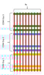
Figure 1. In a zero row sum CDM approach, transmitters in the touchscreen electronics are divided into groups, and each group operates at a different frequency. Control circuitry performs zero-sum measurements on each group. The process cancels out the transmitter signals, virtually eliminating touch-to-display (T2D) interference.
The creation of zero row sum CDM technology was dependent on intensive development of new algorithms. In the past, if you had 20 transmitters, you had to have an algorithm for each possible drive combination. The traditional method of generating these algorithms relies on multiplying the inverse matrix. One of the things that made the development of a zero-row-sum CDM approach profoundly more difficult is that zero-row-sum driving matrices are not invertible (the rank is smaller than the matrix dimension). However, the new approach has a significantly higher signal-to-noise ratio (SNR) at the same frame rate.
Widely applicable
The impact of T2D interference on smartphone manufacturers, and occasionally consumers, is widely known and, to some degree, has been treated as an acceptable loss during the QA process. However, zero row sum CDM provides a solution to this problem.
This article originally appeared in the March’26 magazine issue of Electronic Specifier Design – see ES’s Magazine Archives for more featured publications.