


Low-voltage signals in electrically noisy environments will typically need to be amplified and filtered, whereas others should be excited by an external voltage for applications with varying electrical resistivity. Here Matthew Youngs, Sales And Marketing Manager at Mantracourt, discusses the design considerations of developing high-quality instrumentation amplifiers and signal conditioners.
Modern industrial plants often produce thousands of analogue signals every minute, directly from sensors monitoring conditions such as temperature, pressure, vibration, flow and any other physical parameters required for control and monitoring. This data can be analysed to trigger actions that keep operations flowing safely and efficiently.
Industrial signal conditioning instruments are used to convert the data from these signals into an understandable and universally accepted form, allowing them to be accurately measured. If incoming signals are not conditioned correctly, data measurement inaccuracies will occur and harm system performance levels.
Therefore, it is important that signal conditioning instrumentation is designed and calibrated to accommodate the specific type of sensor it is intended to measure, while also ensuring that signals are properly amplified and filtered. This helps ensure signals are accurately measured and any noise or interference is reduced. As part of this design process, engineers should consider suitable operational amplifiers (op-amp), printed circuit board (PCB) design and enclosure quality.
Amplifier design
The first step in designing accurate amplifiers is choosing the correct op-amp for the input stage. Signal stability must also be established using high-quality gain resistors with temperature coefficients of five parts per million or less.
Potentiometers are often used in amplifier designs to allow for easy calibration. However, because they have poor temperature stability, their range of trim must allow enough adjustment to compensate for variations in the electronic components. In practice, if potentiometer adjustments are too big it will degrade the temperature performance and harm calibration results.
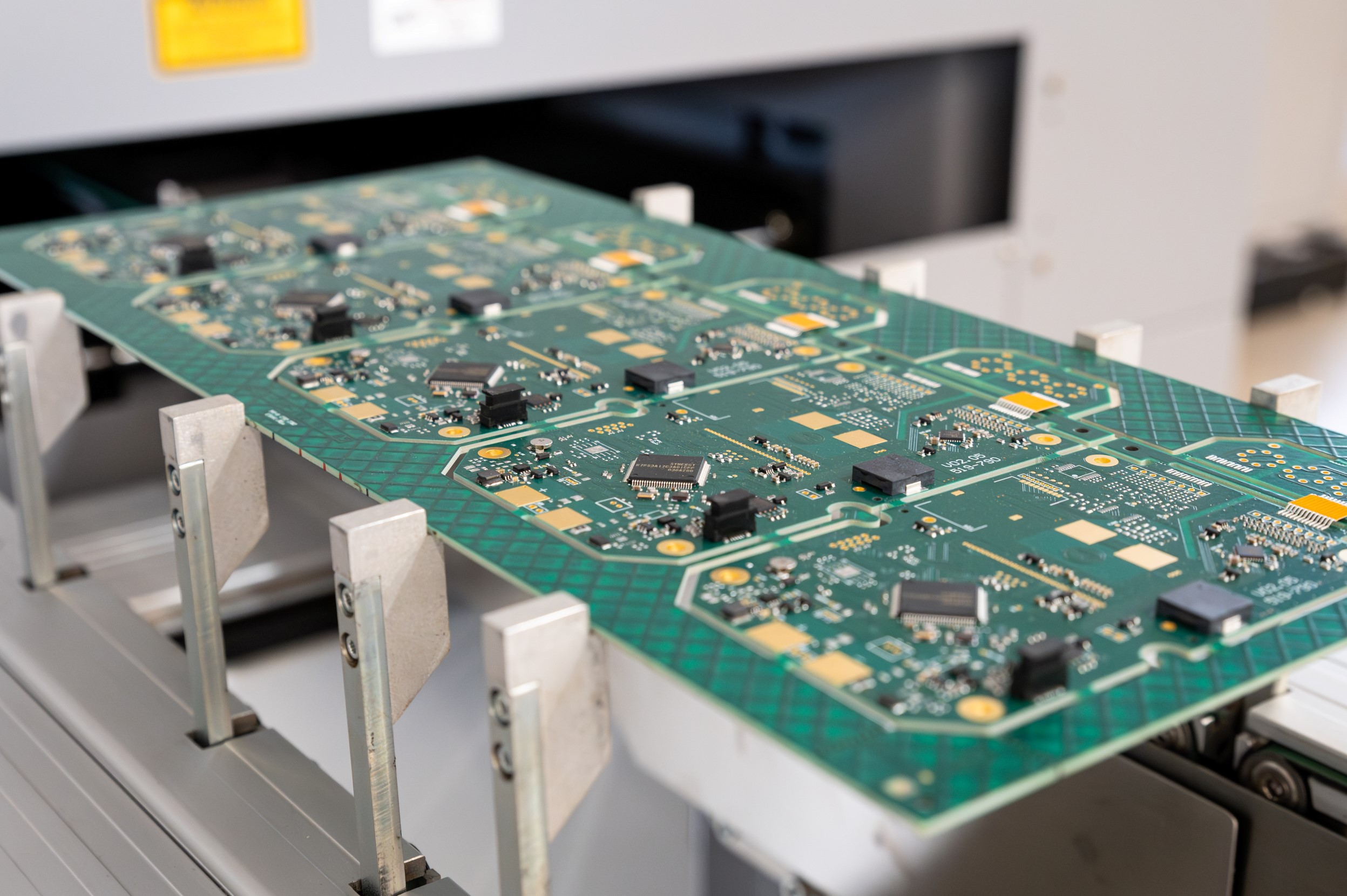
Designing PCBs
For PCB design, engineers must first consider the ground plane, which is usually a layer of copper connected to the circuit’s power supply. Copper is commonly used because it serves as a low-impedance return path for currents flowing from various parts of the circuit. Ultimately, this reduces noise and ensures all components in a system use the same reference potential when comparing different signal voltages.
Furthermore, the ground connection of any component can be directly routed to the ground plane through holes, without running additional tracks. In a similar way to the ground plane, when adopting a multi-layer approach, an internal power plane can be incorporated into the PCB design. Power planes can be placed on adjacent layers to ground planes creating a large parallel plate capacitor that filters the power supply.
High-speed signal transmission will require the installation of guard traces, or tracks, to reduce crosstalk and current leakage. The guard track surrounds a sensitive, high-impedance area of the circuit and connects to a low-impedance source at the same potential. Since there is no potential difference between the guard and the sensitive area, a barrier is formed to any leakage current across the PCB’s surface.
All PCB designs include unintended thermocouple junctions formed by two conductors soldered to copper pads. Unfortunately, because these generate their own thermoelectric voltages, it often modifies the signal voltage. To counteract this, heat sinks and critical components can be placed tightly together. The uniform positioning of components is crucial here. If soldered ends are perpendicular to the direction of heat flow, undesirable thermoelectric effects will be cancelled out.
EMC considerations
The third consideration is to monitor electromagnetic compatibility (EMC) performance. To accurately amplify small signals, stray radio frequencies must be minimised. The problem is that unscreened high-gain amplifier circuits tend to act as radio receivers. Once a stray radio frequency is picked up on resistor legs or PCB tracks, typically it is amplified along with the instrumentation signal.
To overcome this, filters should be included on all I/O lines and PCB tracks should be kept as short as possible. The use of surface-mount components helps in this respect as they have lower resistance and inductance at the connection, meaning fewer stray signals are transmitted.
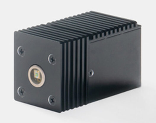
The final factor to consider is the type of enclosure used. Ideally, a fully enclosed metal enclosure should house the signal conditioning module with cable entries using EMC glands. If the enclosure is made using plastic, then additional internal screening should be added, such as copper, to improve conductivity. Furthermore, all wire connections to the amplifier must be appropriately screened. This is especially true for the input wires, which can act as antennas if not properly screened.
By carefully selecting electrical components and taking care when designing PCBs in the way described here, engineers can mitigate against interference and produce amplifiers and signal conditioners that thrive even in the most demanding of applications.
You can learn more about Mantracourt’s range of electronics products on its website here.