


Moore’s law is a prediction made by Gordon Moore, Co-Founder of Intel, in 1965. He observed that the number of transistors on a microchip doubled approximately every year, leading to a corresponding increase in computing power and a decrease in cost per transistor.
This trend has driven the exponential growth in the performance and capabilities of electronic devices, particularly computers, over several decades.
In 1975, Moore revised his observation to predict that the number of transistors would double approximately every two years.
But how long will it last? Moore’s law is reaching its physical and economic limits. As transistor sizes shrink to the nanometre scale (e.g., 5nm, 3nm), fundamental physical challenges, such as quantum tunnelling and increased heat dissipation, make further miniaturisation difficult. These challenges result in diminishing returns in terms of performance and power efficiency. As process nodes shrink, the performance improvements and power savings have become less pronounced. The industry has seen a shift towards optimising other aspects of computing, such as architecture, software, and specialised processors (e.g., GPUs, TPUs), rather than relying solely on transistor density. Also, the cost of developing and manufacturing at the cutting-edge process nodes has skyrocketed. The research, development, and equipment required for each new generation are becoming prohibitively expensive for many companies.
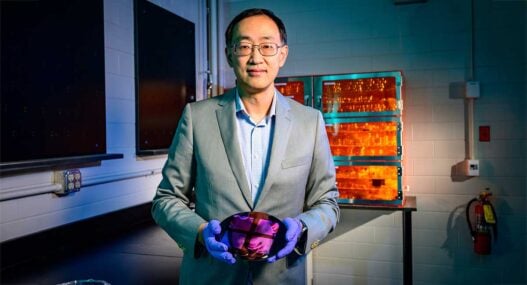
“In a sense, we’re hitting a limit imposed by physics,” said Illinois Grainger Engineering professor Qing Cao. “If you look at the actual size of transistors, they’re not getting smaller, especially in terms of their contacted gate pitch. This is because we’re becoming limited by the intrinsic material properties of silicon and the fundamental rules of quantum mechanics. If we’re going to keep up the trend of increasing processing power of our microprocessors, we have to start thinking beyond just squeezing more devices on a single surface.”
The next leap
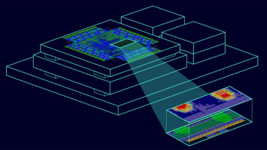
Researchers led by Cao have come up with a promising route to extend Moore’s law without shrinking transistors any further – building upward. The team have demonstrated a scalable way to directly and sequentially stack high-performance silicon circuits. By vertically stacking layers of silicon circuits, chipmakers can dramatically increase computing density and speed while reducing energy use.
Cao explains: “Take something as simple as static random-access memory, which is universal in CPUs and GPUs. Today it takes six microelectronic devices called transistors on a single plane to store one bit of information. With vertical integration, you can distribute them across multiple layers. It’s like replacing a sprawling suburb with high-rises: you get the same functionality, but the spatial footprint is reduced while making communication between layers faster and more efficient.”
The most efficient approach, known as monolithic three-dimensional integration, builds each layer directly on top of the previous one to maximise interlayer connectivity.
The technical hurdle
The core challenge has always been heat. Preparing high-quality silicon and fabricating high-performance devices normally require processes operating at 1,000°C, hot enough to destroy the metal wiring. For upper layers beyond the first, the temperature constraint, or ‘thermal budget’, is strictly set to 400°.
“Generally, the industry accepts that once the first layer of circuits is complete, the thermal budget limit for any additional layers is 400°C,” Cao said. “Researchers in both academia and industry have tried to get around this by working with semiconductor materials other than single-crystalline silicon for the upper layers. But the resulting devices all inevitably suffer from issues with performance and reliability.”
The alternatives that have been explored include polycrystalline silicon, amorphous, or nanocrystalline metal oxides, and nanomaterials such as carbon nanotubes and two-dimensional semiconductors. They all have limitations originating in either intrinsic material properties or extrinsic defects introduced during processing, creating a mismatch between the bottom layer of silicon transistors built on the starting silicon wafer substrate and those upper layers.
What the research achieved
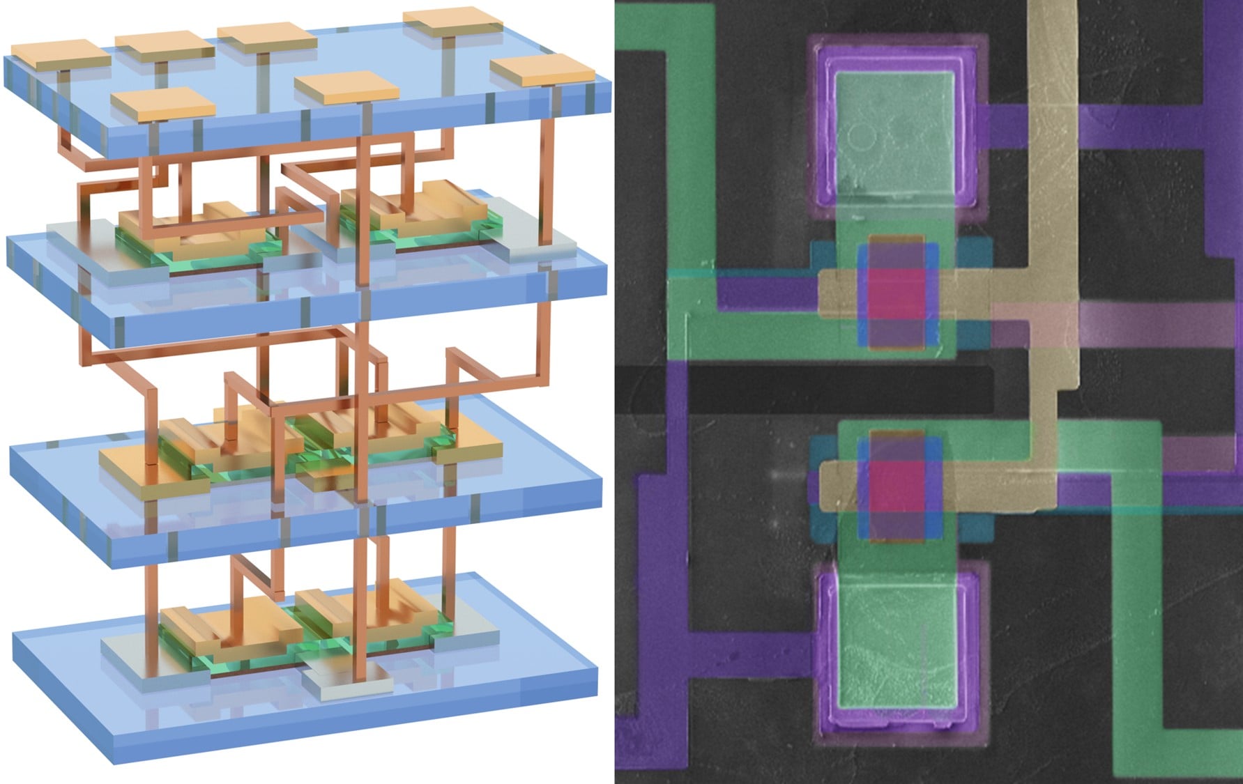
The Illinois team’s breakthrough lies in sidestepping the temperature problem entirely rather than trying to tolerate it. Their process begins by producing ultrathin, freestanding silicon nanomembranes from a donor wafer, which are then transferred onto a substrate already carrying a completed layer of circuits using a roll laminator. The bonding step requires no more than 200°C – well within the 400° thermal budget – while the silicon itself retains its full crystalline quality, and with it the performance and reliability characteristics that alternative materials have consistently failed to match.
“Our method is not only easier to implement with lower cost, but it has several advantages over previous approaches to stack silicon wafers,” Cao said. “The membranes we transferred are only 10 nanometres thick or less, compared to the 500 to 700 micrometres thickness of a typical wafer. Because they are thin, these membranes are mechanically flexible to conform to the underlying surface. This conformality helps avoid interfacial defects like voids, which are common when trying to force two rigid wafers together via wafer bonding.”
Solving the bonding problem was only half the challenge – the team also had to rethink how transistors themselves are built. Conventional fabrication relies on a process called doping, where impurities are introduced into different regions of the silicon to control its electrical properties. That typically requires temperatures above 600°C, making it incompatible with the layers already in place. The researchers’ solution was to switch to junctionless transistors, in which the silicon is uniformly and heavily doped in a single step before the layering begins. The extreme thinness of the films means the gate can still control the channel effectively, while the high doping level keeps parasitic contact resistance low.
The results validate the approach. Across three stacked layers – each containing 625 transistors – the team achieved good yield and uniformity, with output current densities matching those of standard silicon transistors produced at far higher temperatures and running three to four times higher than monolithic devices built from alternative materials. Connecting the layers with vertical metal lines, the researchers went on to demonstrate working three-dimensional logic circuits and static random-access memory cells.
“But most importantly, we’ve shown that this process is scalable,” Cao said. “You can keep stacking layers beyond the three we demonstrated. And the process will yield high-performing transistors with high yield and low variability. We now have a strong foundation for transferring this technology and demonstrating its immediate promise in an industrial semiconductor foundry.”