
Record tunneling magnetoresistance for p-MTJ device
At the 2016 IEEE International Electron Devices Meeting, in a special poster session on MRAM, imec presented a 8nm p-MTJ device with 100% tunnel magnetoresistance (TMR) and coercive field as high 1,500Oe.
This world’s smallest device enables the establishment of a manufacturing process for high-density Spin-Transfer-Torque Magnetic Random Access Memory (STT-MRAM) arrays that meet the requirements of the 10nm and beyond logic node for embedded non-volatile memory applications. It also paves the way for high density stand-alone applications.
STT-MRAM has the potential to become the first embedded non-volatile memory technology on advanced logic nodes for advanced applications and is also considered an alternative to conventional Dynamic Random Access Cemory (DRAM). The core element of an STT-MRAM is a Magnetic Tunnel Junction (MTJ) in which a thin dielectric layer is sandwiched between a magnetic reference layer and a magnetic free layer, where writing of the memory cell is performed by switching the magnetisation of the free layer. STT-MRAMs exhibit non-volatility, high-speed, low-voltage switching and nearly unlimited read/write endurance. However, significant challenges towards commercialisation remain, primarily in scaling the processes for higher densities and in increasing the device switching current.
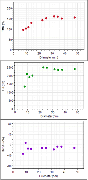
Figure 1 – (a) TMR (tunnel magnetoresistance), (b) Hc (coercivity) and (c) Hoff/Hc (offset field/coercivity, in %) across MTJs of various sizes.
In addressing these challenges, imec scientists have demonstrated for the first time an electrical functional p-MTJ device as small as 8nm. Despite the small dimensions, the device exhibits a high TMR of 100%, a coercivity (Hc) of 1,500Oe and a spin torque efficiency -the ratio of the thermal stability and switching current- as high as three. The p-MTJ stack, featuring a free layer and reference layer of CoFeB-based multilayer stacks, was developed on 300mm silicon wafers and the fabrication process is compatible with the thermal budget of standard CMOS back-end-of-line (BEOL) technology.
Moreover, imec integrated arrays of p-MTJ devices into a 1T1MTJ structure to build STT-MRAM Megabit arrays with pitches down to 100nm, proving that the technology meets the dimensional requirements for the 10nm logic node and beyond.
Product Spotlight
APV1111GVY
Panasonic

Panasonic PhotoMOS® Photovoltaic MOSFET High-Power Drivers
| SKU: | |
|---|---|
| Stock: | 3490 |
| Cost: | $3.95 |
