IDTechEx’s research is designed to help you with that; allowing you to identify and assess existing and emerging markets, to gain deep insights into the business dynamics, to know the key competitors and potential customers, to learn application requirements, and to understand market size and future market potential.
The global market research firm have captured this research in the report ‘Conductive Ink Markets 2020-2030: Forecasts, Technologies, Players‘, which is unrivalled in its depth and breadth. It is based on more than eight years of research. The authors have had first-hand industry experience, and the information herein is based on extensive primary research.
Indeed, more than 150 interviews, 35 conferences and tradeshows, multiple projects, etc. underpin the research. The report covers numerous existing and emerging applications. For nearly every application covered, it describes the market dynamics, assesses the drivers, identifies key technologies, highlights key prototypes and products, mentions vital players, reviews addressable markets, and offers market sizing and projection.
In this article, IDTechEx Analysts briefly discuss applications in automotive, 5G, conformal metallization, and photovoltaics. In subsequent articles the research firm will cover; In-Mold Electronics, stretchable electronics, flexible hybrid electronics, skin patches, 3D printed electronics, printed sensors (piezoelectric, piezoresistive, biosensor, dielectric strain sensors, etc.), RFID, PCB printing, and many other existing and emerging applications.
5G: IDTechEx receive many enquiries about conductive ink opportunities in 5G. There are several interesting opportunities here. First lies in the filter technology, current filter technologies will need to stretch to meet requirements in sub-6GHz 5G and will fall short on mmWave 5G.
A range of candidates are emerging, such as microstrip on PCB or ceramic as well as multilayer LTCC filters. The latter offers reasonable filter properties at mmWave while maintaining a small footprint, which is vital for mmWave 5G implementation where large closely spaced antenna lattices will be used to increase gain and to beam form. It is early days, but multilayer LTCC seems a potential front-runner candidate if tight tolerance can be achieved at high volume production. This would translate into significant paste opportunities.
Another important opportunity lies in highly thermally conductive die attach pastes, e.g. metal sinter or highly loaded epoxies. RF GaN power amplifiers (PAs) are likely to rise as current LDMOS technology will struggle at the required frequencies, even at sub-6GHz 5G. This trend will continue until such point where antenna arrays are large enough to allow Si-based technologies in.
GaN is often attached using gold-based solders, i.e. AuSn, but sinter die attach, or metal (e.g. Ag) filled epoxies can achieve excellent results at a lower cost. Indeed, manufacturers have already qualified such AnSu alternative technologies. As such, this is a growth opportunity.
There are, of course, further opportunities. In particular, minimising transmission loss at high frequencies calls for both low loss materials and minimisation of distances. To realise the latter, more functions are likely to be integrated within a package. This will boost the need for conformal EMI shielding and in-package compartmentalisation. Spray- and inkjet-based approaches are emerging to unseat sputtering. Please see more on this below.
To learn more about 5G, please refer to ‘5G Technology, Market and Forecasts 2019-2029‘. Here, IDTechEx describe and benchmark various filter technologies for mmWave, showing why LTCC is well positioned. They offer 5G forecasts segmented by frequency, discuss and benchmark power amplifier technologies, showing why and when GaN is likely to grow.
They also discuss current methods of die attach and demonstrate why and how metal sintering will become a viable alternative. The report includes a full chapter dedicated to conformal EMI shielding and in-package compartmentalisation.

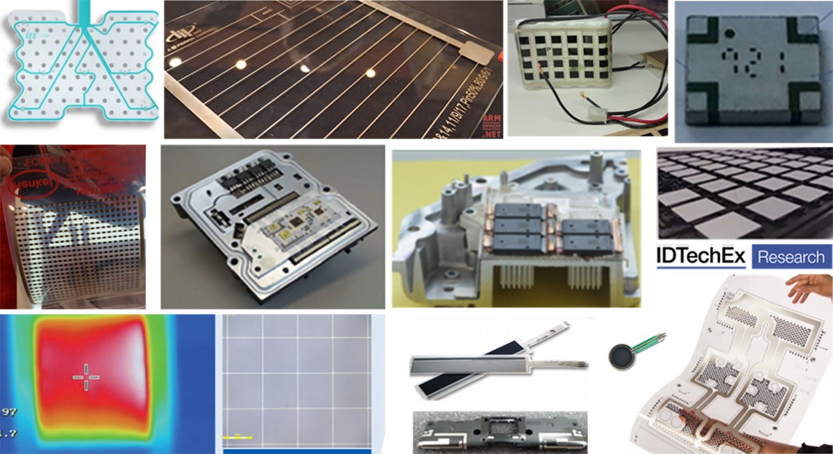
Automotive: The automotive sector has emerged as an important target market for conductive ink suppliers. The traditional applications include printed defrosters, especially on rear-windows. This has been a mature and notable business. A key trend here is to implement transparent and efficient large-area heating to eliminate the visible defroster lines.
Here, printed metal mesh is an excellent candidate, and is already advancing through the qualification process. Furthermore, transparent heating can have other applications, especially in defrosting of perception sensors used in highly-automated and autonomous driving, e.g. cameras or lidar.
Furthermore, seat heaters are also a notable market with ample upside growth opportunity. Printed heating can further expand within the interior of vehicles. Printed occupancy seat sensors and other printed sensors are also an existing opportunity with strong potential upsides.
Electric vehicles and power electronics: Furthermore, the emergence of electric vehicles is a growth opportunity. Printers are developing large-area battery pack heaters to help regulate battery temperatures, especially in cold environments. Importantly, metal sintering die attach pastes have already been commercialised in the EV power electronics.
This trend will continue rapidly as higher power densities, partly boosted by the growing transition to wideband semiconductors, push the operating temperatures beyond the capabilities of many solders. Indeed, the competition here is intense, and many metal sintering material supplies are innovating to offer drop-in form factors, lower sintering time, pressure-less sintering, higher thermal conductivity, etc. This is an interesting space which is analysed in great detail in the report.
There are, of course, other opportunities in vehicles. In-Mold Electronics (IME) is being used to develop both interior and exterior parts, but IDTechEx will cover IME in a subsequent article. LTCC (low-temperature-cofired-ceramics) has long been a commonplace board technology, especially for the ECU, gear control, ABS controller, steer by wire, etc. Last but not least, there can be niche opportunities in electrochromic glass, even in battery EMI shielding.
IDTechEx’s report offers a full analysis of the existing and emerging opportunities for conductive inks in the automotive sector. In particular, it offers a comprehensive yet detailed analysis of the emerging power electronic die attach opportunities in electric vehicles.
Electronic Packaging and conformal metallization: There are multiple aspects of this trend. Aerosol printing had gained some popularity in mobile phone direct-on-part antenna production and similar. This opened a market for mono-disperse nanoparticles. The rise of 5G will likely put such designs at risk. Furthermore, some products have reached the end of the cycle. As such, the defining question will be whether aerosol can find new applications beyond mobile phone antennas.
Conformal EMI shielding is a megatrend which will accelerate in the coming years. Here, we see a transition from low cost but bulky lid-based board-level shielding to thin conformal package-level shielding. This trend is not exactly new, and one of the early adopters was the application processor on the 2015 Apple watch.
Many components today in mobile phones have conformal EMI shielding. In general, the most common elements are WiFi, Bluetooth and other RF front end modules. Conformal coating on NAND memories is rarer but increasing.
Sputtering is the well-entrenched processes here. It benefits from being proven and from sunk CapEx investment. It, however, may not have the highest Unit Per Hour (UPH) rate given that sputtering rates will need to be slowed to achieve good adhesion to the epoxy molding compounds. This approach uses a SUS-Cu-SUS structure and is thus light on bill of materials. Instead, it is heavy on machinery costs as multiple sputtering tools will be needed.
Multiple ink-based alternatives are now emerging. Spraying is one option. Here, the process is non-vacuum. The ink composition and particle morphology do matter. The thicknesses here are 3-6um, and good side and top thickness uniformity are obtained. The ink-jet based approach is novel. It uses particle-free inks activated by light exposure. Here, there will be no nozzle clogging.
The suppliers are suggesting that they can achieve sufficient shielding at just 1-2um thickness with UHP reaching 12k on 10mm2 packages. In both approaches, Capex is low, making the technology accessible to all manners of OSATs and lower value ICs and applications. This can, in the longer term, boost volumes.
In general, ink-based approaches can only partly conformably cover the package, leaving some areas unexposed. Furthermore, jetting can also be used to fill in trenches created to isolate parts within a package, leading to in-package compartmentalization. This is a critical attribute, especially when antenna-in-package designs, important for 5G, are considered.
For more information about aerosol as well as package-level conformal shielding, please see the report ‘Conductive Ink Markets 2020-2030: Forecasts, Technologies, Players‘.
Photovoltaics: This remains the largest market worldwide for firing-type pastes. This is an irreplaceable market volume-wise. Indeed, the PV market has been roaring ahead since 2014, more than doubling in size. Indeed, global installations are expected to have exceeded 114GW in 2019. However, this is not an easy market for paste or powder suppliers. Here, price pressures are immense and performance advantages temporary and short-lived. Only those with large and well-established production lines can participate.
Non-silicon wafer-based PV technology is now confined to very small niches in the market. These, nonetheless, represent important sales opportunity, especially in forming the electrodes. This opportunity extends mainly to thin and highly conductive lines which cured at low temperatures. Such requirements match well with what nanoparticle inks seek to offer.
This report covers the dynamics of the silicon PV industry. It looks at historical, current, and future trends. It examines industry learning curves, price evolutions, installation capacities, leading produces, dominant cell architectures, etc. It also examines trends in conductive ink technology and supply chain. Furthermore, it examines various thin film PV technologies, including CIGS and solution processed organic PV.


