


In this article, Mark Patrick, Mouser Electronics will investigate data converters’ architectures, look at how these converters work, and explain the key terminologies engineers should review when selecting a converter. A selection of typical analogue-to-digital (ADC) and digital-to-analogue converters (DAC) illustrate the different converter architectures and showcases their capabilities.
Connecting the analogue and digital worlds
The world around us is analogue. Environmental factors such as temperature, humidity, and air pressure are analogue measurements. To process them in a home automation system, for example, we need to convert them into the digital domain. Processing information digitally is a convenient, quick, and power-efficient process, for which low-cost microcontrollers are ideal.
The opposite of an analogue to digital conversion process is a digital to analogue function. Some application use cases utilise both conversion methods; for example, an intelligent home speaker must listen for spoken commands and playback responses. Converting human speech into a digital audio stream is then interpreted by a cloud-based machine learning algorithm, actioned, and the answer or the desired music is sent back to the speaker for conversion to the analogue domain.
How ADCs and DACs work
Figure 1 illustrates a simple, functional block diagram of an industrial process closed loop controller featuring an ADC and a DAC. The figure highlights that signal conditioning functions support the ADC and DAC on their input and output. Signal conditioning may involve using low pass filters on the ADC input, for example, to remove any high-frequency signal artefacts from the desired analogue signals that might interfere with the ADCs conversion accuracy. Other signal conditioning components might limit the input range of the acquired analogue signal to prevent damage to the ADC and an isolation circuit to isolate the sensors from the ADC or DAC galvanically.
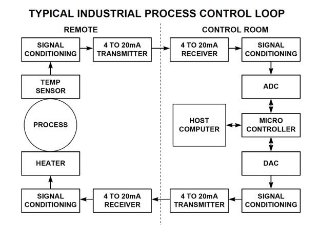
Figure 1: The use of an ADC and a DAC in an industrial process loop controller (Source: Analog Devices)
Where multiple analogue sensor elements are utilised, the input to the ADC can be multiplexed, providing a cost-efficient approach to a control circuit’s design. The design might require a programmable gain amplifier to accommodate different analogue input ranges from multiple sensors (Figure 2).

Figure 2: A complete analogue to digital to analogue control loop with a microcontroller or microprocessor (Source: Analog Devices)
ADC and DAC functions may be designed using a discrete component approach. However, the most time-efficient and PCB space-effective method is to select an integrated circuit (IC) that typically includes the ADC or DAC functions, a multiplexer, and some signal conditioning components.
An introduction to analogue-to-digital conversion
The basics of data conversion involve two distinct processes, sampling, and quantisation.
Sampling occurs in a continuous time domain and determines how faithfully the digital output signal represents the input analogue signal. For slow-changing analogue signals, a slow sampling rate is sufficient, but an input that is changing rapidly requires a faster sampling rate (Figure 3). Sampling is typically quoted as the number of samples per second (s/s).
In Figure 3, towards the right-hand side, the analogue input signal changes much quicker than the sampling rate, resulting in a loss of conversion accuracy.
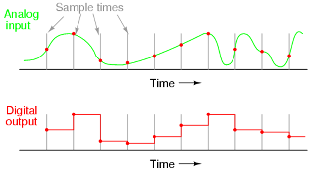
Figure 3: The impact of sampling rate on the reproduction of a digital output signal (Source: Kuphaldt –http://www.ibiblio.org/)
Quantisation determines the analogue value for each digital bit. The resolution is the second fundamental attribute of selecting an ADC. For example, an 8-bit ADC can represent the input signal in 256 levels, but a 16-bit ADC improves the resolution to 65,536 steps, so each digital bit represents 256 analogue values compared to an 8-bit ADC. In general, the use case determines the selection criteria for the ADC’s resolution and sampling rate (Figure 4).
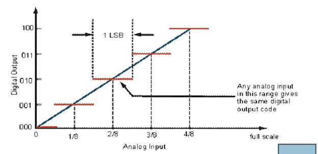
Figure 4: The quantisation process determines the value of each digital bit and the ADC’s resolution (Source Analog Devices)
Digital conversion basics
The same concepts of sampling and quantisation also apply to digital-to-analogue conversion. Each quantised value is created from a binary digital code. Typically, the simplest DAC employs a binary-weighted architecture to provide an output signal, using a voltage divider constructed with high precision resistors (Figure 5). This architecture is termed a string DAC.
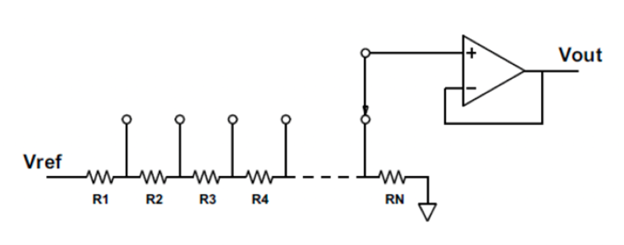
Figure 5: Using a string of precision resistors to create a voltage divider to create an analogue output from a digital input (Source: Analog Devices)
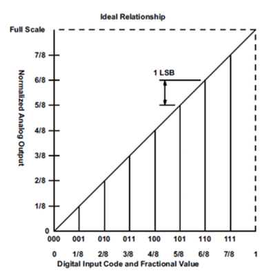
Figure 6: The analogue output of a 3-bit DAC is normalised to a digital fraction (Source Analog Devices)
Essential datasheet ADC and DAC terminology
In addition to the sampling rate and quantisation highlighted above, these are some additional terms you will encounter when selecting ADCs and DACs.
Resolution: Quantisation determines the resolution of a DAC/ADC and is best illustrated as the analogue value of a digital bit. Consider measuring a voltage with a maximum value of 5VDC. In an 8-bit ADC, the least significant bit (LSB) equates to 19.5mV (5/256) compared to a 16-bit yield 76µV (5/65,535).
Integral Nonlinearity error (INL): This error represents how much the converter’s linearity departs from a straight line through the range from zero to full scale. A good INL indicates that the converter could convert a digital sine wave, for example, into a faithful analogue representation (see Figure 7).
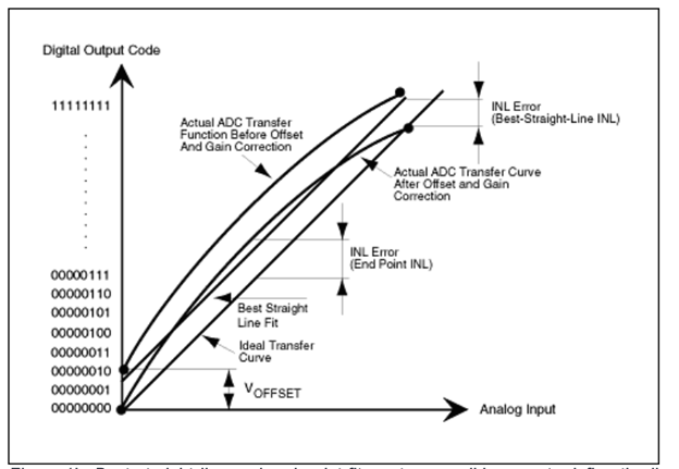
Figure 7: An illustration of a line of best fit of an ADC compared to overall transfer function (Source Analog Devices)
Gain error: A gain error indicates how accurately the slope of the transfer function mirrors the ideal transfer curve (Figure 7).
Differential Nonlinearity error (DNL): DNL indicates the difference between each digital step. A good DNL means good resolution with the digital steps as uniform (Figure 8).
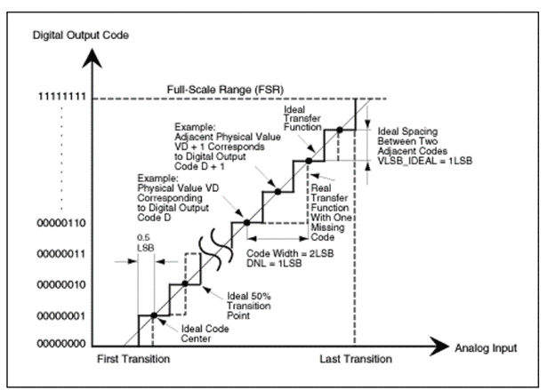
Figure 8: The differential nonlinearity error exists between each digital step (Source: Analog Devices)
Offset error: Also referred to as the zero-scale error, it indicates how well the transfer function of an ADC or DAC compares to the ideal transfer characteristic. In a DAC, an offset error occurs when an analogue output occurs when the digital inputs are all zero. For an ADC, all digital outputs should be zero when the analogue input is zero
Popular ADC and DAC architectures
Analogue to digital conversion
Each analogue to digital converter architecture has attributes that make it suitable for specific use cases with the principal factors influenced by cost (simplicity of design), resolution, or linearity.
A flash architecture employs a parallel array of clocked comparators to convert an analogue signal into the digital domain. Each comparator is fed with the input signal and a set fraction of a reference voltage from a resistor ladder (Figure 8). A flash architecture achieves conversion within one clock cycle. However, it requires eight comparators for an 8-bit ADC, which also imposes a high input capacitance.
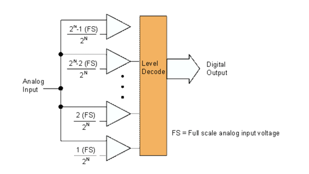
Figure 9: The outline architecture of a flash ADC (Source: Analog Devices)
A pipelined architecture typically divides the conversion process into two stages, each consisting of a sample and hold, a DAC, and an ADC. At the start of a conversion cycle, the first sample becomes the most significant bit (MSB), which is then fed back and subtracted from the input signal with the residual sampled. The process continues for each bit from MSB to LSB. This architecture is not as fast as a flash ADC, but it can accommodate a wide dynamic range of input signals and achieve a high resolution. However, the pipelining process introduces conversion latency which might not suit some applications.
The successive approximation register (SAR) architecture compares the input signal against a known reference voltage (Figure 10). It continues to make comparisons against successively smaller reference voltages for each digital bit, from MSB to LSB. Each bit is set if the analogue input is greater than the reference; if not, it remains zero and continues to the next bit. The advantages of a SAR ADC include no pipelining delay and, since only one comparator is required, the die size is kept compact. However, accuracy depends on the DAC linearity and any comparator noise.
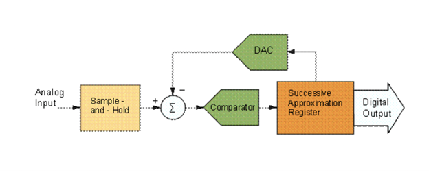
Figure 10: An outline of the successive approximation analogue-to-digital converter (Source: Analog Devices)
A sigma-delta architecture utilises an integrator, comparator, and a one-bit DAC to create a sigma-delta modulator (Figure 11). The modulator subtracts a value from the DAC and feeds the result to the integrator. The comparator takes the integrator output and converts it to a single-bit digital output, which is fed back to the input. This architecture yields a high resolution and can operate at a fast ‘oversampling’ rate.
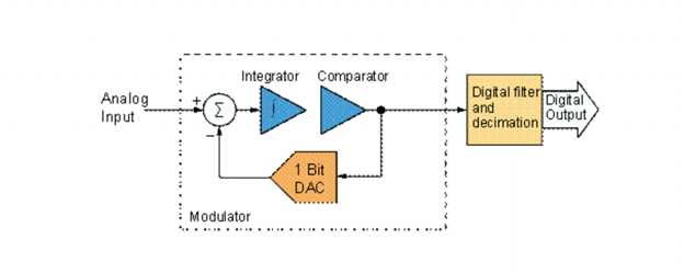
Figure 11: The architecture of a sigma-delta ADC (Source: Analog Devices)
Digital-to-analogue conversion
In addition to the string architecture highlighted above, an R-2R ladder DAC is another popular architecture (Figure 12). The R-2R ladder simplifies the resistance-matching challenges associated with a string DAC, with just two resistor values in a 2:1 ratio required. The architecture suits voltage or current output configurations. In a voltage mode R-2R DAC, resistors are switched between a reference voltage and ground. Each chain of the resistor ladder provides a binary-scaled output voltage; the summed total becomes the analogue output.
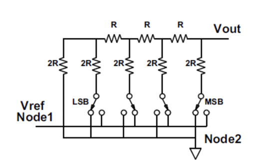
Figure 12: The basic architecture of an R-2R ladder DAC (Source: Analog Devices)
All the DAC architectures described so far use a fixed reference voltage and a fixed gain. However, the multiplying DAC (MDAC) architecture provides a digitally variable gain to a wide dynamic range analogue signal. It uses an R-2R ladder and a programmable gain op-amp. This approach offers the ability for the MDAC to function as a DAC-based attenuator or amplifier and is ideally suited to high bandwidth AC or varying DC signals.
Data converter showcase
The Texas Instruments ADC354x series are low noise, ultra-low power 14-bit high-speed ADCs capable of achieving up to 65Ms/s. With a latency of one clock cycle, a 900MHz input bandwidth, an INL of +/- 0.6 LSB and a DNL of +/- 0.1 LSB, the converters suit a wide range of low-power applications such as software-defined radio, thermal imaging, and instrumentation.
An example of a SAR-based ADC is the Analog Devices AD7380/AD7381 series of 4Ms/s dual sampling 16- or 14-bit converters. Differential inputs, a 1 LSB INL (14-bit), and a wide common-mode input voltage make the converters suitable for motor control sensing, data acquisition systems, and sonar applications. An evaluation board, EVAL-AD7380FMCZ/EVAL-AD7381FMCZ, aids multi-channel, simultaneous sampling prototyping.
An example of a DAC is the Analog Devices/Maxim Integrated MAX22007. This four-channel analogue output IC suits various industrial and building automation applications. Capable of configuration as either voltage or current mode outputs, each channel can provide a 0V to 10.5V linear output voltage or a 0mA to 21mA linear current.
The Texas Instruments DACx3401-Q1 is a compact 8-pin WSON packaged, automotive-qualified DAC. Available in 8-bit or 10-bit variants, the devices offer 1 LSB INL and DNL linearity, a wide operating supply voltage range (1.8VDC to 5.5VDC), and a low power 0.36mW @ 1.8V consumption profile.
Getting started with data conversion
In this short article we’ve investigated how data conversion between the analogue and digital domains is achieved, given a quick introduction to key datasheet terminology, and looked at popular converter architectures. Equipped with this information, readers will have a better understanding of how analogue-to-digital converters and digital-to-analogue converters operate, some pros and cons of each architecture, and the key datasheet specifications to review when selecting a device.