
FPGAs address rising complexity of MIPI-based vision
Today’s embedded vision system designers must address a number of market trends. For example, current designs feature an ever-rising number of sensors to collect higher levels of data or perform new functions. Take the average automobile as an example, and it's here that FPGAs can play a key role.
A couple of decades ago, auto manufacturers were considered innovative when they added a single backup camera. Today those same manufacturers are using cameras for lane departure monitoring, speed sign recognition and a host of other smart driving applications.
At the same time embedded vision system designers are migrating to components compliant with the Mobile Industry Processor Interface (MIPI) Alliance. Originally developed for the mobile market, MIPI defines the hardware and software interface specifications mobile device designers need to build high performance, cost effective and reliable mobile solutions.
Over the last few years MIPI has become the dominant standard for building embedded systems. Designers across a growing array of applications, including the industrial and automotive arenas, have taken note and are now looking for ways to capitalize on the high performance and economies of scale afforded by mobile components.
Escalating time-to-market pressures are driving demand for easy-to-use, embedded vision solutions as well. Supplying a chip alone is no longer enough. These pressures continue to drive designers to embedded vision design environments that offer all the hardware, software, IP and reference designs they need to quickly design and develop end products.
At the same time, the current generation of users expect a responsive, consumer-like experience with their embedded displays. Embedded displays that are slow to boot up show visual artifacts that can disrupt the user experience.
New obstacles
While these rapidly escalating trends bring opportunity, they also present serious obstacles to embedded vision designers. First, the cameras and displays used in many embedded systems do not match the type or number of interfaces on today’s application processors (APs). APs offer a limited number of I/Os for sensors. APs also need to support a wide array of display and sensor types. This is complicated by the fact that display sizes and resolutions vary based on their application.
Moreover, given their long lifespan, many industrial displays currently in use were originally designed to connect to displays via legacy interfaces. How can designers in embedded applications leverage the advantages of the MIPI component market when their designs rely on the use of legacy or proprietary displays and sensors?
To support the use of more sensors and more efficiently manage I/O resources, designers need a programmable solution that can compensate for the limited availability of I/Os. Ideally such a solution would offer the ability to aggregate sensor inputs and allow the designer to pre-process data to offload processor overhead.
An ideal solution would also be programmable to allow designers to easily adapt to customized display designs. In the past designers could only support different display sizes and resolutions by developing a custom ASIC for each display type. A programmable solution would allow designers to support different custom display requirements with a single device.
Lattice Semiconductor led the industry in this effort in 2016 with the introduction of CrossLink™ FPGAs, a programmable video bridge that supports a wide variety of protocols and interfaces for mobile image sensors and displays.
To address the evolving needs of the embedded video market Lattice has announced a new enhanced version of CrossLink called CrossLinkPlus. To address user demand for seamless display bootup, CrossLinkPlus adds 2 Mbits of flash embedded on the device as configuration memory.
With its on-chip flash memory, CrossLinkPlus can boot up in less than 10 ms so visual artifacts don’t disrupt the user display experience; the human brain can’t perceive images that disappear in under 15 ms. The on-chip flash can also be used to support in-field reprogramming.
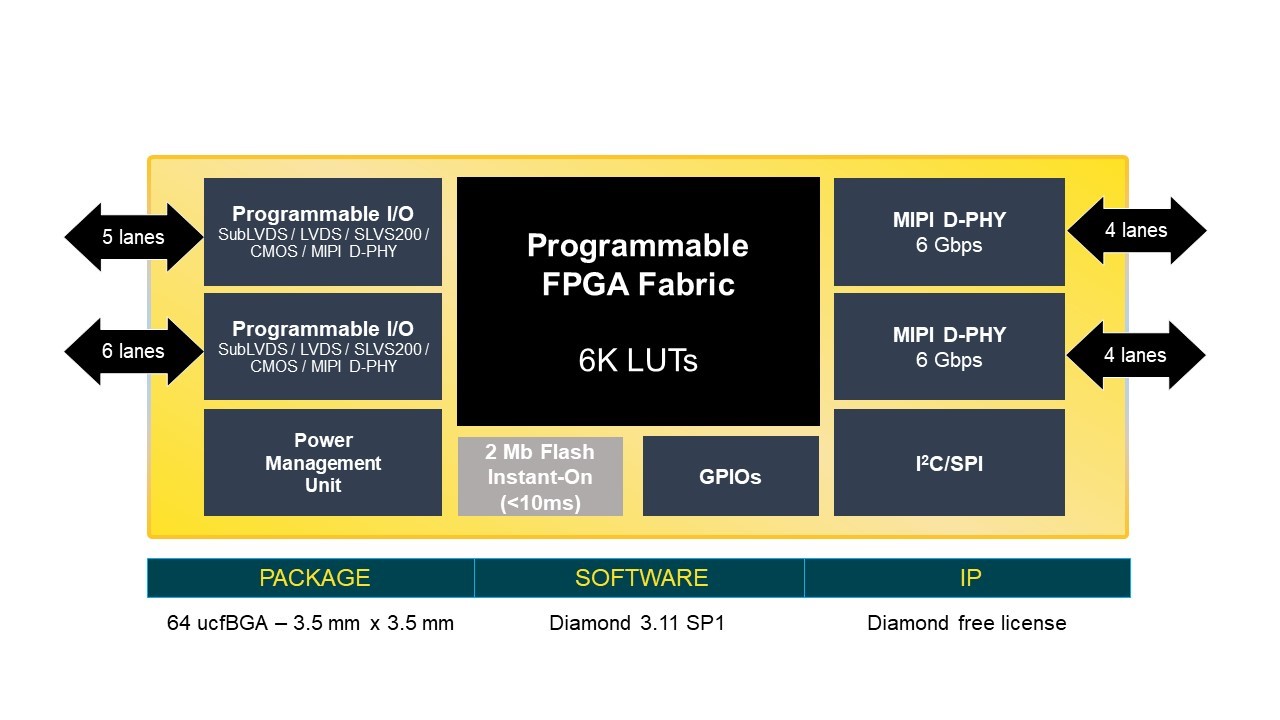
Figure 1: Lattice Semiconductor’s CrossLinkPlus FPGA
CrossLinkPlus offers the fastest MIPI D-PHY for its size while keeping power consumption low. The FPGA delivers a combined 12 Gbps D-PHY performance in a 3.5 x 3.5-mm package. Besides its high speed MIPI D-PHY, CrossLinkPlus adds a 6K LUT programmable FPGA fabric and flexible high speed I/Os that support video bridging across MIPI CSI-2, MIPI DSI, LVDS, SLVS200, CMOS and Sub-LVDS interfaces. The ability to interface to these displays and sensors offers design teams a high degree of design flexibility.
To address rising time-to-market pressures, the new device promises to help development teams improve design efficiency. For instance, a comprehensive library of ready-to-use, pre-verified IP for receiver, converter and transmitter functions allows designers to focus on the value-added features of their design that differentiate it from competitors. Pre-verified video IP blocks and reference designs not only shorten the design cycle, they are also free and available immediately. Moreover, the IP blocks are completely reusable across the CrossLink and CrossLinkPlus product families.
Lattice also offers easy-to-use hardware and software tools that simulate functional behavior, validate system-level functions, and accelerate product development. Having flash memory embedded on the device allows designers to address rapidly changing market requirements by field-upgrading new bitstreams to the flash. The new and enhanced CrossLinkPlus also helps engineers meet more aggressive space and thermal constraints without the power consumption associated with external flash.
From a competitive standpoint, the device delivers the fastest-in-class hardened MIPI D-PHY speed per unit area. In a comparison of similar devices from industry competitors, Lattice’s CrossLinkPlus offers better D-PHY performance in a smaller footprint than competitors and lower power consumption.
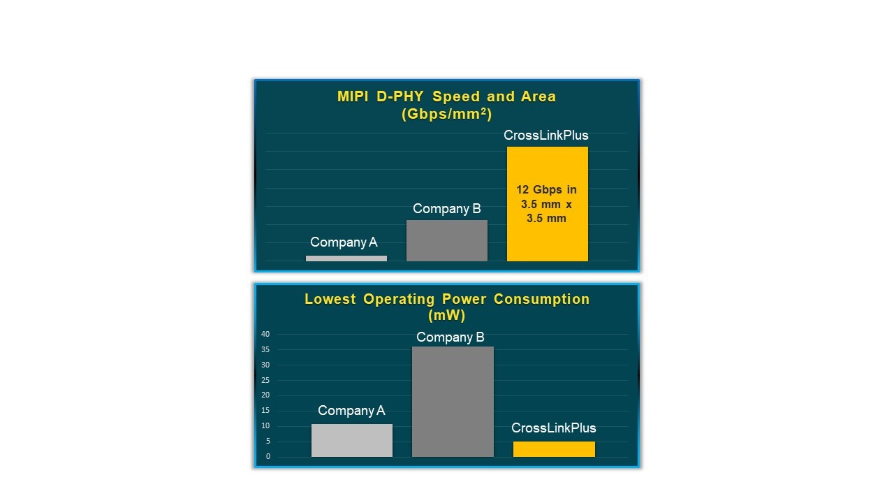
Figure 2: Lattice’s CrossLinkPlus FPGA provides a high-performance MIPI D-PHY while still maintaining very low power consumption.
Lattice offers extensive support to accelerate product development. For example, Lattice regularly introduces new reference designs for CrossLink and CrossLinkPlus. These reference designs tailor to the most in-demand video bridging features for new and existing product designs.
New applications
Popular use cases of the CrossLinkPlus showcase the high degree of design flexibility it gives designers. Figure 3 below depicts how the device can be used to bridge between sensors and processors with different interfaces. In this case the designers are presented with a problem: on the one hand they want to take advantage of the cost, performance and footprint advantages typical MIPI processors offer. At the same time, they want to retain the capabilities of a legacy camera built to industry standards. In the machine vision application in Figure 3, designers would address this by using the CrossLinkPlus to bridge between a legacy camera featuring a Sub-LVDS interface and a MIPI processor featuring a D-PHY interface.
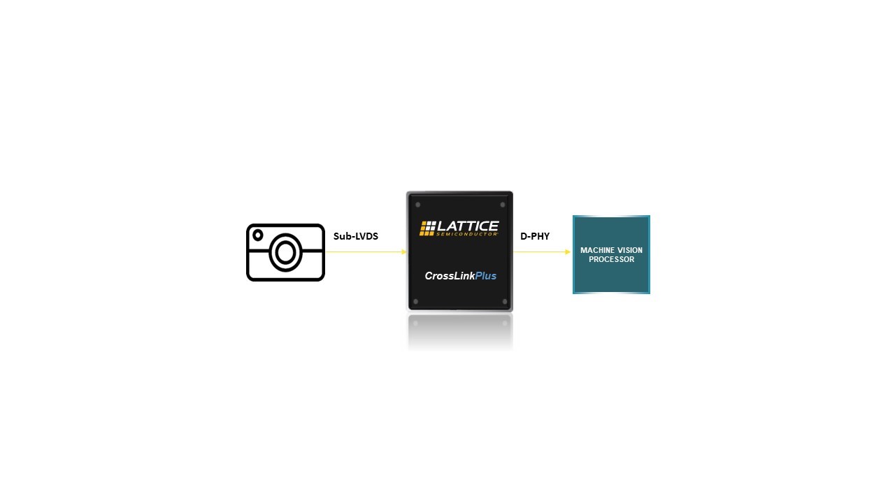
Figure 3: In this application example, the Lattice CrossLinkPlus FPGA serves as a bridge between a Sub-LVDS camera and the MIPI I/O on the device’s machine vision processor.
A second potential use for Lattice’s CrossLinkPlus is to aggregate the input of multiple sensors back to the application processor. For example, in Figure 4, three image sensors interface with a CrossLinkPlus device via three D-PHY ports. CrossLinkPlus aggregates the sensor data into a single D-PHY output to the processor. This aggregation capability allows designers to optimize use of their processor’s often limited I/O resources.
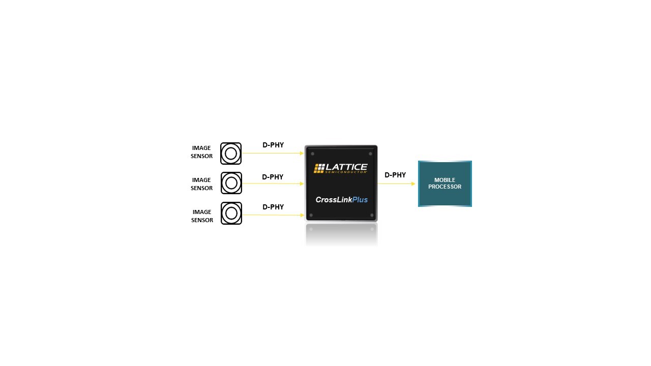
Figure 4: Lattice CrossLinkPlus can aggregate multiple sensor signals over one port to conserve processor I/Os.
Designers can also use CrossLinkPlus to implement a MIPI signal splitter or duplicator. In Figure 5, designers feed a signal from a sensor into the CrossLinkPlus device and then split the output or duplicate it across two separate outputs. Lattice sees this approach increasingly used in automobile ADAS applications for smart cars or in applications where data redundancy is important. In this use case, a signal coming from a camera enters a Lattice CrossLinkPlus device and is copied to two output streams.
One stream is sent to an applications processor that processes data in real-time. The second stream is archived to localized or cloud-based data logging and backup, much like an airplane’s black box. If there is a failure or car accident, investigators can go back to the data backup to determine what caused the event.
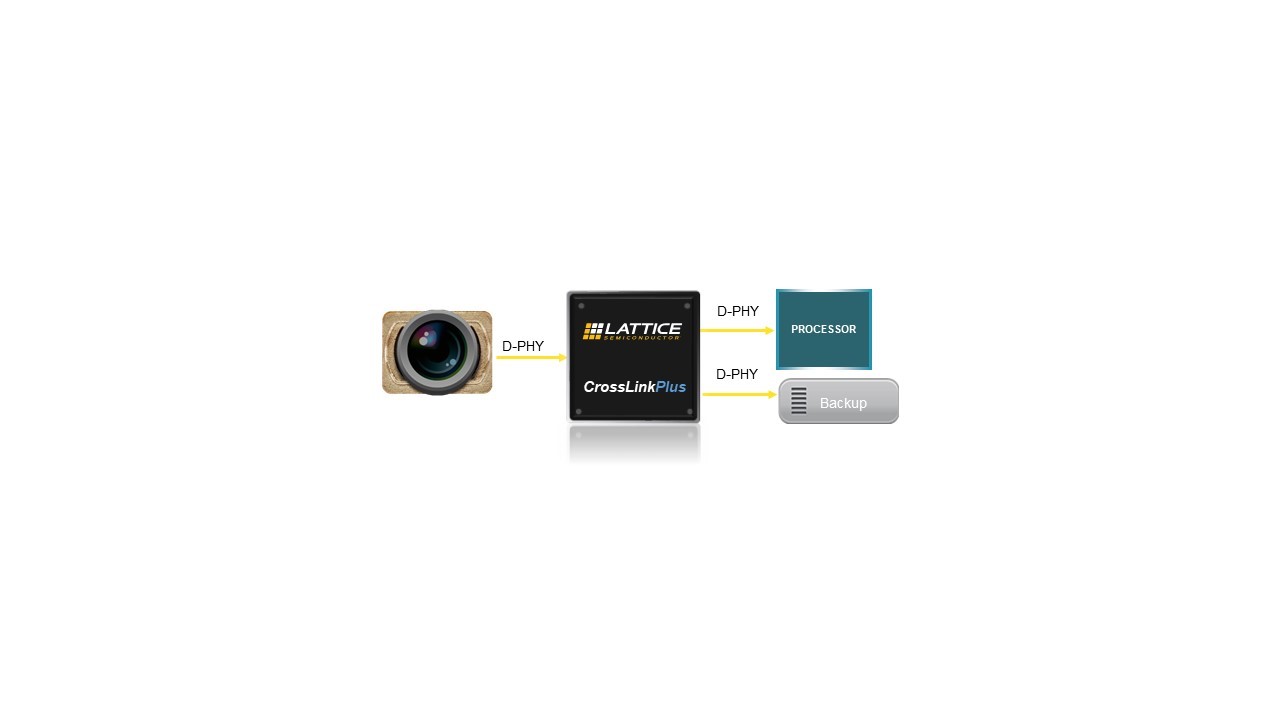
Figure 5: In this ADAS vision system, the CrossLinkPlus FPGA is duplicating the camera signal output to send to both the application processor and a data backup.
Figure 6 below illustrates how designers can use CrossLinkPlus to link a legacy display to a new higher performing AP. Many industrial control applications need a bridge to connect between an AP and a legacy display using OpenLDI, as OpenLDI displays are typically much bigger than MIPI displays. The new MIPI applications processor delivers data to the CrossLinkPlus device via D-PHY. The device then bridges the data to the legacy display using OpenLDI. Similarly, CrossLinkPlus can be used to bridge connections between non-MIPI image sensors and a MIPI AP.
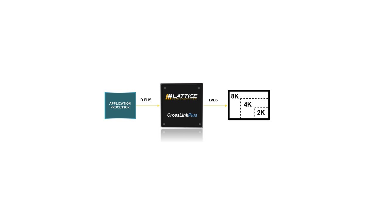
Figure 6: In this application example, Lattice CrossLinkPlus is enabling a connection between a legacy display and a modern application processor.
Conclusion
Today’s designers searching for a new way to accelerate embedded vision development need to look no further than Lattice’s CrossLinkPlus. By bringing FPGA reprogrammability to embedded vision systems, CrossLinkPlus allows designers to capitalize on the cost and performance benefits MIPI components offer.
Its hardened D-PHY interface offers industry-leading performance, while its embedded flash memory enables instant-on display performance. Its low power operation and compact footprint help simplify thermal management and its support for an array of popular and legacy interfaces maximizes design flexibility.
Finally, CrossLinkPlus’s comprehensive, pre-verified and free IP library speeds development and allows designers to spend more time focusing on the most important part of their design -- their competitive advantage.

Featured products

MAX17793
Analog Devices Inc.

3V to 80V, 3A, High-Efficiency, Synchronous Step-Down DC-DC Converter
| SKU: | MAX17793 |
|---|---|
| Stock: | 9316 |
| Cost: | $3.64 |

MAX22516
Analog Devices Inc.

IO-Link Data Link Controller with Transceiver and Integrated DC-DC
| SKU: | MAX22516 |
|---|---|
| Stock: | 8000 |
| Cost: | $5.42 |
Product Spotlight
102991834
BeagleBoard

Single Board Computer (SBC), BeagleY-AI
AM67A BeagleY-AI Jacinto 7 AR...
| SKU: | 2820-102991834-ND |
|---|---|
| Stock: | 183 |
| Cost: | $56.24 |
SC1110
Raspberry Pi

Raspberry Pi 5 2GB
The Raspberry Pi 5 2GB model represents a leap for...
| SKU: | 2648-SC1110-ND |
|---|---|
| Stock: | 185 |
| Cost: | $38.33 |
AKX00069
Arduino

Arduino Plug and Make Kit
The Arduino Plug and Make Kit features the ...
| SKU: | 1050-AKX00069-ND |
|---|---|
| Stock: | 945 |
| Cost: | $66.97 |
300361-0011
Molex

MX150 Mid-Voltage MatSealed Female Connector Assembly, Dual Row, 20 Circ...
| SKU: | |
|---|---|
| Stock: | 280 |
| Cost: | $2.51 |