


When the luxury of many signal and power layers are available to a PCB designer, there is far more flexibility to route the signals and to deliver multiple rails of power to support these very high-speed signals and processors. In a four-layer PCB, this task is especially challenging due to the limited number of power and signal layers available to the designer.
Much research has been done and many papers have been published stating that it is necessary to have closely spaced power and ground planes in order to provide power plane capacitance to supply switching current at very high speeds to wide parallel buses such as PCI and DDR. Yet, these same buses function properly in four-layer PCBs that do not have any detectable interplane capacitance. Examples of products that function at very high data rates with four-layer PCBs are most desktop PCs as well as high-performance game consoles.
Figure 1 illustrates a typical stack up of a four-layer PCB with the planes L2 and L3 close to the outer layers, so that the signals on the two outer layers have correct desired impedances. Because of this build up, the distance between the two planes is fairly large, in this case 48 mils (1.2mm). But to create any useful plane capacitance, the plane separation must be less than 4 mils (0.1mm). So, the question arises: how can a high-speed design work with such a stackup? This design guide is intended to answer that question.
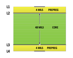
Figure 1. A typical four-layer PCB stackup
The design problem
The problem that first arises when a high-speed design does not have adequate interplane capacitance to support the switching-current transients associated with modern logic systems, is EMI failure due to the high-frequency energy radiating from the product. If the lack of capacitance is severe, logic failures can also appear.
To understand the source of this problem, it is useful to examine what occurs when high data rate signals switch from a logic 0 to a logic 1. Most CMOS logic signals are series terminated as shown in Figure 2.
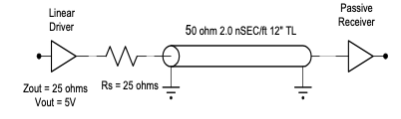
Figure 2. A typical series terminated CMOS logic signal
When a logic state switches from 0 to 1, there is a requirement for current or charge from the power supply system. Figure 3 shows the voltage waveforms at the driver output (red) and at the load or input (yellow) for the circuit in Figure 2. As the signal travels down the transmission line, its parasitic capacitance is charged up to Vdd by transferring charge from the power system capacitance to the line capacitance.
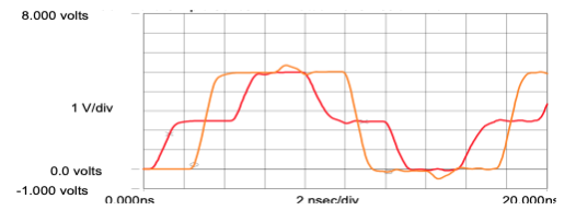
Figure 3. Switching voltage waveforms for circuit in Figure 2
The diagram in Figure 4 is the current waveform that must be supplied by the power distribution system (PDS).
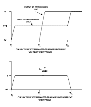
Figure 4. Switching voltage and current waveforms when going from logic 0 to logic 1
To understand the frequencies that make up the current waveform in Figure 4, one must convert from the time domain to the frequency domain, and this is accomplished by using a Fourier Transform. Figure 5 shows a Fourier Transform of the switching waveform for the circuit in Figure 2 which has a clock frequency of 30MHz.
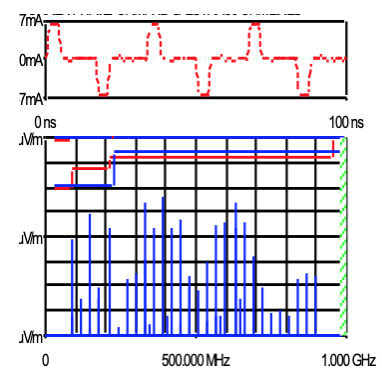
Figure 5. Fourier transform of current waveform in Figure 4
The red waveform at the top of Figure 5 is the current waveform, with the positive-going excursion illustrating the current being drawn from the PDS when switching from 0 to 1, and the negative-going excursion illustrating the charge being removed from the parasitic capacitance of the line while switching from 1 to 0. Notice that the first frequency is about 85MHz, it is not a harmonic of the 30MHz clock frequency, and there are no harmonics of the 30-clock frequency in the spectrum.
Traditional EMI rules suggest that EMI is a function of clock frequency, however the transform in Figure 5 shows that this is not true. The events that make up the frequency spectrum in Figure 5 are as follows: the lowest frequency in the spectrum will be set by the round trip delay of the transmission line, and the highest frequency will be set by the rise time of the signal.
Those who have experienced EMI failures may recognise the spectrum in Figure 5. The reason is, if the PDS capacitance is not capable of supplying this charge, there will be voltage variations (ripple) on VDD with this frequency spectrum. Any CMOS output that is at a logic 1 shorts its transmission line to VDD, hence these variations will appear on that line. If this line exits the product, it will quite simply serve as an antenna, radiating its energy into space and thus causing the EMI failure.
Solving the EMI problem
The PDS will need to be redesigned if an EMI problem such as above occurs when providing the charge needed at the frequencies involved in the switching event. This means that physical capacitors with sufficient capacity must be added to the PDS so that when charge is drawn from them to support the switching activity, the drop in voltage (ripple) is small enough to eliminate the EMI problem.
If a system fails EMI, this is a red flag that the power delivery system does not have enough of the right kinds of capacitors to support the switching events during normal operation.
The frequency at which a capacitor is useful as a source of charge is determined by its value and the parasitic inductance inherent in connecting it to the PDS. The problem we have is that all real capacitors perform at a narrow band of frequencies limited by the parasitic inductance inherent in their design, in addition to the inductance added when connecting these capacitors to the power planes in the PDS.
Figure 6 shows the equivalent circuit of a typical capacitor. Notice that there are three components involved: ESL is the equivalent series inductance of the capacitor (to which the inductance of the mounting structure must be added); ESR is the equivalent series resistance of the capacitor (and its mounting structure) and C is the capacitor itself. This combination is often called a series-resonant circuit.
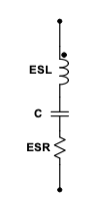
Figure 6. Equivalent circuit of a capacitor
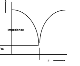
Figure 7. Impedance vs frequency of the capacitor in Figure 6
Figure 7 is the impedance vs frequency of the capacitor in Figure 6. Notice that at both low and high frequencies the impedance is very high. The bottom of the curve is called series resonance. At the one frequency the reactance of the inductance and the capacitance cancel each other, and the resultant impedance is the ESR or equivalent series resistance. It is at this frequency that it is easiest to deposit charge onto the capacitor and extract it to support the switching events. At values above and below the series resonance, the capacitor is unable to participate in the switching activities.
The middle right curves in Figure 8 are a plot of the impedance vs. frequency for the 1uF, 0.1uF and 0.01uF capacitors commonly specified in most applications notes from IC manufacturers. Notice that the 1uF capacitor is series resonant at about 5MHz, the 0.1uF capacitor is series resonant at about 18MHz and the 0.01uF capacitor is series resonant at about 40MHz. These frequencies are applicable to the capacitors before they are mounted onto a PCB. The mounting structures necessary to connect them to the power planes will add additional inductance, driving the series resonant frequencies even lower.
None of the commonly specified capacitors can supply the frequencies seen in Figure 5, resulting is excessive ripple on VDD, hence possible EMI problems.
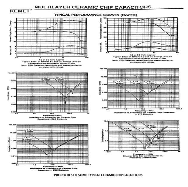
Figure 8. Impedance vs frequency of 0.1uF and 0.01uF capacitors
Solving the inadequately performing capacitor problem
The forgoing discussion has shown that the capacitors usually specified in application notes cannot provide the high frequency switching currents required by high-speed logic circuits. The following presentation was made by Todd Hubing and his staff when they presented the problem and its solution.
Power Bus Decoupling on Multilayer PCBs, by Todd Hubing, etal, IEEE Transactions on Electromagnetic Compatibility, Vol 7, Number 2, May 1995.
In this paper it was shown that the solution was to add interplane capacitance to the PCB to supply the charge needed by fast switching circuits. Why does interplane capacitance work when discrete capacitors do not? The answer is that the parasitic inductance of closely spaced plane pairs is far lower than what discrete capacitors can achieve. As a result of this observation, PDS engineers have been designing PCB stackups to guarantee enough interplane capacitance to support all the fast-switching events in a design. Calculating how much interplane capacitance is needed is discussed in Reference 1 noted at the end of this paper.
Replacing the missing interplane capacitance in four-layer PCBs.
Referring to Figure 1 the two planes are so far apart that there is little if any interplane capacitance. How, then, can such a stackup support very fast switching events on buses such as DDR and PCI?
Processor and memory IC manufacturers such as Intel and AMD have known about this problem for a very long time. And they have solved the issue by providing the needed capacitance to support these switching events on the IC package and on the die itself. One needs to consult the IC data sheets and applications notes in order to determine whether or not such capacitance has been provided in the devices themselves. Most of the other suppliers of ICs such as FPGAs, have not done this. As a result, designs containing these types of ICs will not work on a four-layer PCB. Recently however, some of the FPGA manufacturers have begun to add capacitors in the die and package so as to make their devices function better on four-layer PCBs.
Additional comments on adding interplane capacitance
Figure 9 shows the stackup of a typical six-layer PCB. The left image depicts the stackup as originally designed, where the product failed EMI tests due to a lack of interplane capacitance. The right image depicts the same stackup after adding copper fill in the unused areas of the four signal layers.
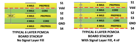
Figure 9. Six layer PCB stackup before and after adding signal layer fill
Figure 10 shows the artwork for the six layers with the signal layer fill added. The copper fills applied to each of the four signal layers are in turn attached to appropriate power rails, so that the copper fill power plane is close to an opposite polarity power rail on the adjacent PCB layer, thus creating an interplane capacitor that was not there before. In this way we have created five capacitors as shown on the right side of Figure 9, as opposed to only one as shown on the left side of Figure 9. The result could possibly be an increase in plane capacitance from only 0.5nF to more than 4nF.
Figure 11 depicts the before and after results of an EMI scan of the PCB shown in Figure 10. The blue frequencies show the EMI before adding the signal layer copper fill shown in Figure 8 and the red frequencies are the EMI after adding the signal layer copper fill.
Some caution needs to be exercised though when applying this kind of signal layer copper fill. Notice that in Layer 3 the added copper fill is adjacent to signals in Layer 4. Clearly, this will alter the impedance of the trace in L4, sometimes to such as extent that it may create a signal integrity problem. Hence if impedance matching is important on a trace or group of traces, one should rather avoid filling the adjacent layer with copper.
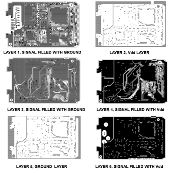
Figure 10. Six layer PCB artwork layers showing signal layer fill
Caveats when designing high-speed four- or six-layer PCBs
The interplane capacitance associated with closely spaced power and ground pairs provides a very low impedance between the two layers. When a stackup has multiple power and ground layer pairs, all of the ground layers will be connected to each other wherever there is an interconnecting component ground pin. Each VDD plane is effectively connected to its respective ground layer with the interplane capacitance, such that all of the planes are connected to each other at the AC frequencies contained in the switching signals. It is thus possible to change signal layers when routing, without a concern that the return currents will have a path from plane to plane. Similarly, when a signal crosses a split in a VDD plane (such as to accommodate two or more VDD voltages in the same plane), there won’t be a problem.
Please note that in a four-layer PCB with no plane capacitor, this does not apply. In this case, in order to have a continuous path for the return current, the signal traces must begin and end on the same layer and they must not cross any plane splits.
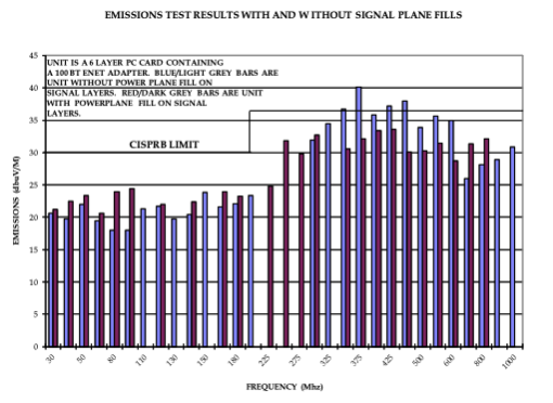
Figure 11. Before and after EMI scan for the PCB in Figure 9
Summary
By following these carefully created guidelines, it is indeed possible to replace high layer count PCBs with four-layer PCBs. And for today’s high-speed and high-performance electronics product demands, this solution can be a much more efficient and cost-effective approach.
Event tip
Author and PCB design guru Lee Ritchey will be holding a face-to-face high-speed design seminar near Frankfurt, Germany, on 6-8 December 2022. Engineers interested in this 3-day hands-on event can find more information and registration details at https://www.leonardyseminare.de/p/high-speed-course-face-to-face-lee-ritchey-december-06-07-08-2022.
Reference materials
- High-speed PCB and System Design, Volumes 1 & 2, Lee Ritchey, and John Zasio.
- Power Bus Decoupling on Multilayer PCBs, by Todd Hubing, etal, IEEE Transactions on Electromagnetic Compatibility, Vol7, Number 2, May 1995.
- Principles of Power Integrity for power Delivery System Design, Prentice Hall, Larry Smith, and Eric Bogatin 2017.