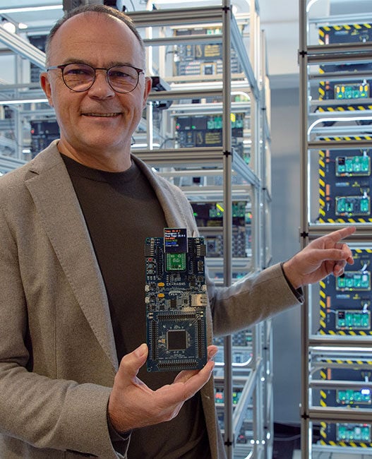


Here, Steven Lee, Product Manager at Keysight EDA, and Dr. Nicola Femia, Professor at the University of Salermo, discussed various topics ranging from SiC and GaN to the challenges in implementing these new power solutions.
The current trends in power electronics
The key trend currently sweeping power electronics is the rise of wide bandgap technologies, something that Keysight themselves are actively working to bring continual solutions to.
Wide Bandgap (WBG) semiconductors, such as Silicon Carbide (SiC) or Gallium Nitride (GaN), are currently emerging technologies but are swiftly moving as a more mainstream approach, especially in industries like automotive. “The trend is currently towards using wide bandgap materials in our electronics across various industries… They operate at higher voltages, higher temperatures, and have lower switching losses, which improves overall efficiency,” explains Lee.
The technical superiority of WBG semiconductors lies in their ability to reduce energy losses and enhance overall device performance, particularly in high-frequency applications. Continues Lee: “These materials, they have their high-level wider bandgap and traditional materials like silicon. So, it really allows them to operate higher voltages and higher temperatures and also lower switching losses and overall losses with higher efficiencies because that’s what it’s all about when it comes to power conversion, right? We’re trying to squeeze every single point 1% out of that conversion. You know, I think this is going to continue to evolve and we’re going to see gallium nitride and silicon carbide becoming more and more used in the industry.” Keysight expects integral current and future industries to see a significant impact from this technology, particularly in the EV automotive, renewable energy (solar/wind in particular), aviation, and industrial machinery industries.
Size is also a growing trend within this space, traditional methods mean that core components of power converters end up being somewhat bulky and cumbersome. By utilising SiC and GaN WBG semiconductors you can reduce the overall footprint of these products whilst simultaneously lowering overall costs.
Challenges that come with WBG semiconductors
However, whilst the benefits of WBG semiconductors are great on paper, in application there are a myriad of challenges that must be overcome before widespread adoption can occur. These challenges are the driving force behind a cautious approach in adoption, as outlined by Dr. Femia: “We must be very careful with wide bandgap because the risk is that we get trumped in the fascination for new technology that is not well understood.”
The challenges can be broken into three key areas, these are:
- Layout challenges: Layout parasitic effects are a constant problem in these devices, and are only amplified by the faster switching speeds offered by SiC and GaN approaches. “When it comes to layout, the parasitic elements of parasitic inductance, parasitic capacitance, can introduce unexpected effects… even a little bit of inductance can cause voltage spikes that create performance issues,” says Lee. Hence, it is important to design circuit layouts that can manage these parasitics without compromising the device’s overall performance.
- Thermal challenges: Thermal management is critical to the integration of WBG semiconductors into power electronics as the high power density and efficiency of these materials can lead to significant heat generation, requiring new approaches to cooling. “As part electronic designers, we really do look at thermal challenges… we’re always trying to cool down our transistors. With WBG materials… the thermal management becomes even more critical due to their ability to operate at higher temperatures,” explains Lee. Device selection, safety and reliability under specific operating conditions, heat sink solutions, operating condition estimations, and interface material selection are all integral to addressing the thermal challenge posed by these materials.
- EMI challenges: The high-frequency operations of WBG semiconductors mean that EMI complications are a must-address to ensure proper functionality. Explains Dr. Femia: “All the EMI issues that you have with the standard power converters using silicone or even silicone carbide devices are multiplied with the use of GaN, this is because the same PCB inductance or capacitance can become prohibitive at a certain signal rate of current and voltage this approach achieves.” The other concern is that the EMI generated is internal, and thus harder to measure and manage.
What’s next?
Despite these challenges, the future remains bright for the emerging technology that is WBG semiconductors, and the ongoing advancements taking place from companies like Keysight are becoming increasingly transformative. As we look to the future, the potential of WBG technologies like SiC and GaN offers a promising horizon, with proactive efforts in addressing design challenges setting the stage for more robust and efficient power electronics across various industries.