






An AI agent that can respond to problems and repeat steps on its own is now doing part of the work of designing a computer chip. But the decisions that matter most – what a chip is used for and which compromises are acceptable – still belong to engineers, says Rod Metcalfe, Senior Product Management Group Director at Cadence.
Chips sit inside everything from phones to data centres. How quickly and reliably they can be designed matters far beyond industry; it spills into the lives of everyday people.
Here, we look at what AI does in chip design today, where engineers still make decisions, how its work is checked, and what customers have measured. Note that the figures cited in this article come from Cadence and its customers and are not from independent testing.
Designing a chip involves defining what it should do, turning that into circuitry, checking that it works, and making sure it can be manufactured. AI is helping at some of these stages, but at different levels of maturity, says Metcalfe.
What AI does today
Chip design, says Metcalfe, is the next step in the long evolution of chip design. “Decades ago chip design migrated from netlist capture to RTL synthesis, which enabled much larger and complex designs to be created in significantly less time,” he says. When it comes to AI, he sees it as part of the same pattern: “AI is just the next stage in this design abstraction journey.”
Machine learning is already used to explore design options and improve power and performance. Agentic AI can go a step further; it “can use engineering tools, check their results, and decide on the next steps,” Metcalfe says. In the early, or front-end, stages of design, Metcalfe says that agents can generate hardware descriptions, create verification plans, run tests, and investigate failures. Cadence’s ChipStack AI Super Agent applies this approach to chip design and verification, while its InnoStack AI Super Agent covers digital implementation and 3D-IC (stacked chip) design.
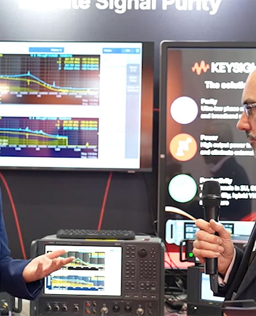
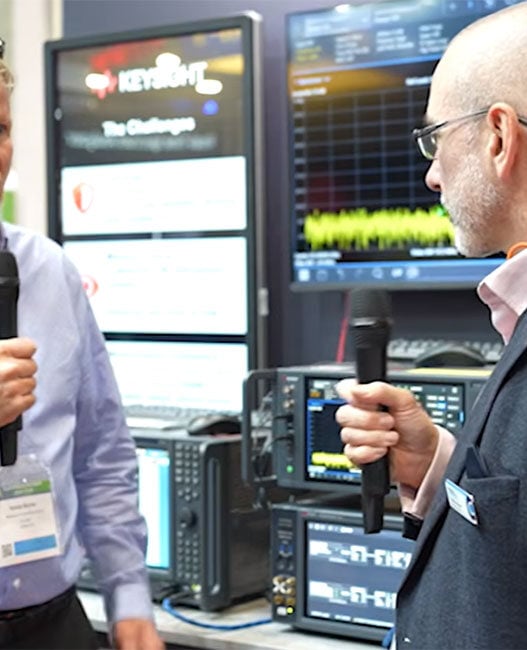
At Microelectronics UK 2026, Metcalfe demonstrated an agent handling digital implementation, which is turning a design into a physical layout. It responded to challenges of converting the design code into circuitry and deciding where blocks sit on the chip on its own, and repeated steps when needed: “This shows the difference between just following instructions and adapting the workflow based on results.”
A multi-die system, which combines several pieces of silicon in one package, shows what that adaptability can mean in practice. Moving components around can change both electrical behaviour and temperature, so the two have to be analysed together, he says. Agent-based workflows can make those changes and run the right simulations, which helps teams compare options and find problems sooner.
The decisions AI can’t make
Metcalfe says that when it comes to AI in semiconductor design, the decisions that remain with engineers are the ones about purpose and compromise. “People still need to decide what the product is meant to achieve and what compromises are acceptable.” That covers how much performance is enough, what the limits are on power, cost, and space, and what happens if something fails.
Engineers must also question the specification itself. A tool can optimise against requirements it is given, but those may be incomplete or may conflict, particularly when a chip is part of a larger system.
Agents can take on a good deal of the execution and exploration, says Metcalfe, but only inside the limits that people set. “Experienced engineers are still responsible for defining the boundaries, interpreting conflicting results, and deciding whether the evidence is sufficient to release the design.” Their role, he says, is expanding to include directing and assessing the agents’ work.
A mistake found after a chip has been made can cost a great deal of time and money. Generated code has to be tested against the specification using simulation and, where suitable, formal verification, which uses mathematical methods to check that a design meets the required properties under set assumptions. The physical design must also meet timing, power, electrical, and manufacturing requirements at sign-off, the final check before a design goes to manufacture.
Metcalfe says that the agents he describes are connected to established design and verification tools, and this is what makes their work testable. “The engineering tools provide a way to test the agent’s work against something more dependable than another generated answer,” he said. Teams can also use one language model to produce the design and a different one to check it against the specification.
This does not remove the need for judgement. Engineers must still review assumptions, constraints, test coverage, and open issues. “A passing result only covers what was actually checked.” He says that faster automation should let us check more, but it shouldn’t lower the standards for final design sign-off.
What this means for engineers
This is what Metcalfe describes as a move towards engineers stating the result they want and spending less time on each manual step. Part of that move is talking to software in plain language, but he says this has limits. “Talking to software in natural language helps, but it doesn’t fully replace the use of engineering tools.” Both traditional and agent-based ways for working will continue, and adoption will vary.
Metcalfe expects repetitive scripting, setup, and coordination to take less time. Knowledge of architecture, verification, and how parts of a system interact becomes more useful, because engineers need to spot results that look good but hide problems. AI “cannot reliably identify every issue on its own,” he says.
It is also interesting, he says, to see how junior engineers, who do not yet have much design debug experience, can use AI agents “to become more proficient in complex debug tasks.” His advice to those starting out is to learn both the tools and the engineering principles behind them “so they can confidently oversee AI automation.”
Complexity and the limits of AI
Chips now pack in smaller components, stacked layers, and several pieces of silicon in a single package. AI doesn’t make that complexity go away. Metcalfe points out that AI “helps us tackle specific design problems in complex systems, but it can’t change the basic physics.” Heat, power delivery, connectivity, mechanical stress, and manufacturing remain challenges.
What has changed, however, is how much of the design space engineers can explore and how soon they see the effect of a choice they make. It is not only about coping with complexity; Metcalfe says, AI also “helps engineers find better solutions.” Yet this still depends on accurate simulation, solid constraints, and engineering knowledge.
What to the numbers show?
In a 90-day evaluation covering three key design blocks, Tenstorrent reported up to a fourfold speed-up in verification using Cadence’s ChipStack AI Super Agent. Altera reported roughly a tenfold reduction in verification effort in some areas.
In early evaluations of its RTL (register-transfer level, a way of describing a chip’s behaviour in code) Generation Agent, Cadence reported average reductions of 24% in area and 18% in power compared with RTL produced by a general-purpose AI model alone. Cadence’s recent announcement with Nokia describes a fivefold speed-up of targeted design and analysis workflows, using its AuraStack AI Super Agent and Millennium M2000 Supercomputer. Socionext, which is deploying InnoStack AI SuperAgent, is aiming for a fivefold productivity gain in physical design for large 3nm chips.
Metcalfe says: “I see these as specific reported results, not industry averages or guarantees for every project.” The verification gains apply to specific tasks, not whole chip projects, and the RTL result does not claim an improvement over every engineer-led process. The figures also do not show a direct cut in size, total cost, or time to manufacturing. He says that his measurement of success is “the quality of designs and how quickly they can be delivered.”
What holds adoption back
Trust and protection of intellectual property matter, but adoption also depends on workflow, says Metcalfe. Teams need to know a new tool fits with their existing tools, design data, review processes, and computing set-up, and that the benefit justifies the effort.
Design holds valuable proprietary information, so customers want to know where data is processed and who or what can reach it. One way to do this is to connect the agents to language models through a secure gateway instead of giving external services direct access. Another is on-premises deployment, which Metcalfe says Nokia uses to keep agents, tools, and computing within its own environment.
For teams that are starting out, Metcalfe advises to “start with a clear task and a measurable baseline, agree on what proof would show success, and then build from there.”
Who benefits and what it costs
Metcalfe thinks AI could benefit small and large companies alike. A small team could automate repetitive work and try more options, while larger firms have more computing resources and can roll out new methods across many projects. The customer stories show big gains are possible, he says, but they don’t prove which company size benefits most. He expects easy-to-use, well-integrated tools to matter most, and sees real opportunity in “more teams to take part in design,” provided costs and deployment options work for smaller groups too.
On cost, he says the possible savings come from less repeated engineering work, earlier detection of problems, and reaching production-ready design sooner. These have to be weighed against the cost of software, computing, and integration. Less engineering effort could make some custom-chip projects more appealing, but fabrication, packaging, validation, and volume still shape the business case. “Faster design doesn’t automatically make every custom chip affordable, but it does help with one key part of the equation.”
AI agents are already taking on part of the work of designing a chip, from generating hardware descriptions to adapting a physical layout when results change. But the choices that matter the most – what a product is for, which compromises are acceptable, and whether evidence is strong enough to release a design – stay with the engineers making them. The gains described by Metcalfe are real, but they apply to specific tasks rather than whole projects, and a passing result only covers what was actually checked. For teams weighing up where to begin, Metcalfe’s advice is to start small and have a clear task and a measurable baseline. A faster design “doesn’t automatically make every custom chip affordable, but it does help with one key part of the equation.”