


While the world has looked on with excitement at the technical progress of 5G, designers are now busying themselves with how to power the base stations to make it happen. Core to 5G’s future success is its trilogy of target capabilities: tremendous throughput, ultra-low latency, and massive connectivity. Compared to 4G base stations, which provided a competent downlink but were more lacking in the uplink, 5G base stations’ improved uplink capability alone demands more power. The planned higher throughput and number of subscribers supported by each base station only adds to the challenge. In addition, there are practical issues regarding infrastructure placement.
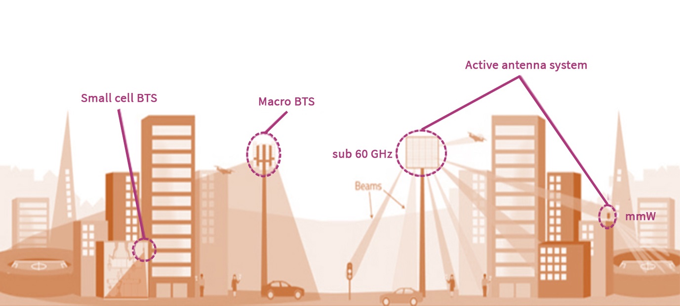 Figure 1: Small cell base transceiver stations and active antenna systems for 5G connectivity.
Many base stations are installed in or on property rented for the purpose and have limits on floor area, volume, and allowable install weight. The move to 5G demands that equipment remains within these limits. Additional micro base transceiver stations (BTS) and active antenna systems (AAS), covering the sub GHz and millimeter wave (mmWave) spectrum, are needed to provide the coverage and capacity for massive connectivity (Figure 1). These require rental of new sites that will also be subject to severe weight and volume limits and may also have a cap on available power. A trend to wall and pole mounting is also expected, along with integration in existing utilities, such as street lighting. The financial aspect plays a role here too. The rental of suitable locations has a significant impact on operational expense (OpEx), making up more than one third of the outlay. If smaller, lighter, and more power-efficient base stations enable cheaper rental costs and lower utility bills, marginally higher capital expenditure (CapEx) for the radio equipment and power supply can be accommodated.
Cellular infrastructure
Studies show that energy costs make up between 10 % and 15 % of OpEx in mature markets. In developing markets, especially those with a high proportion of off-grid, battery-powered sites, this rises close to 50%. As little as 15% of the energy delivered is used for the transfer of data bits between base station and handsets, 35% goes into redundancy systems while 15% is dissipated in power supplies and fans. The personnel costs associated with maintaining sites are the second largest portion of OpEx and China Mobile has linked power supply issues to 70% of downtime cases, putting robustness and reliability in focus.
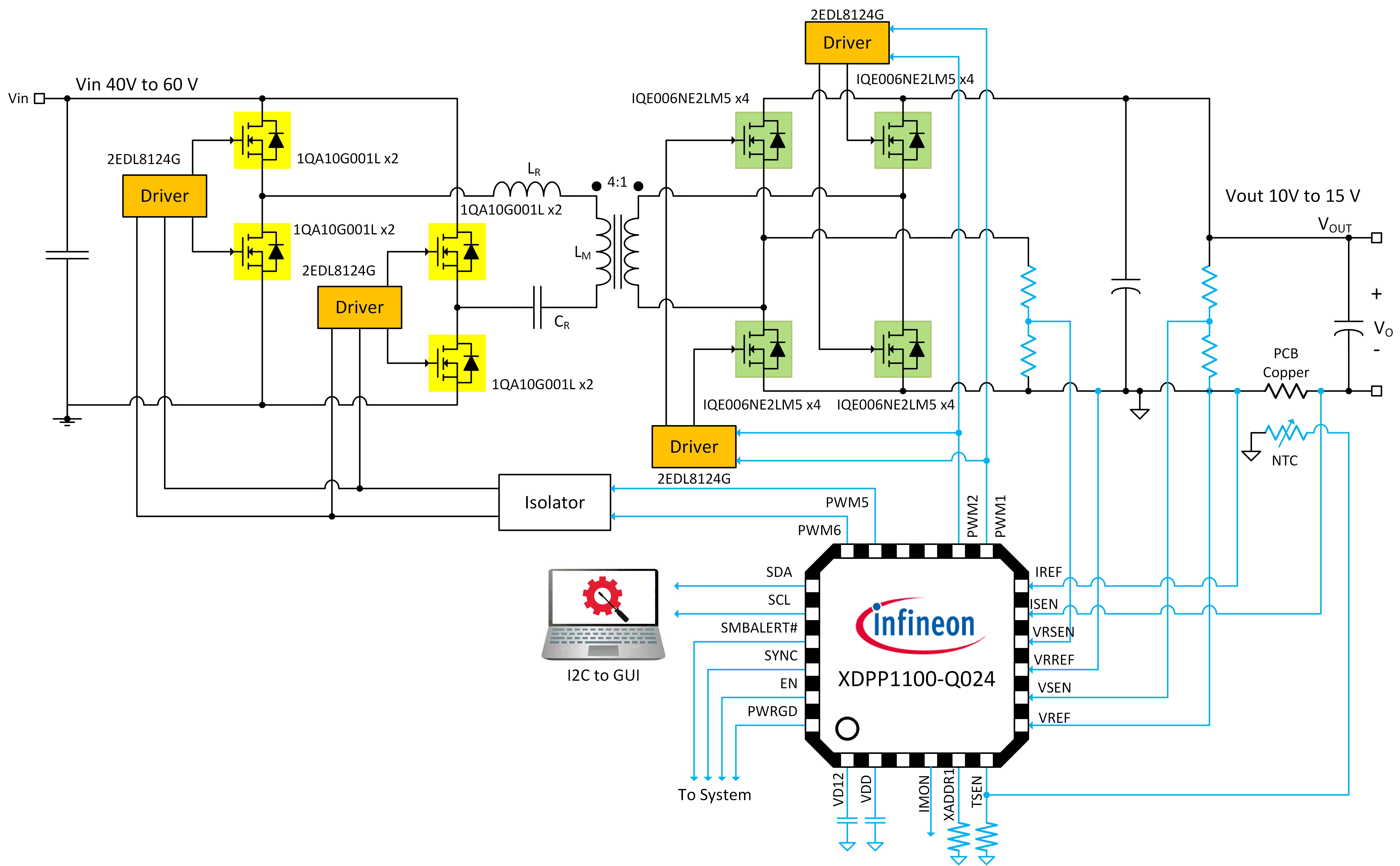 Figure 2: Fixed frequency 1kW DC/DC LLC is used to compare efficiency improvement of CoolGaN over silicon MOSFETs.
Silicon power device performance has incrementally improved over the years, but the arrival of wide-bandgap (WBG) technology, such as gallium nitride (GaN) offers power converter designers an improvement that can be applied to their products.
GaN high electron mobility transistors (HEMTs) offer a relatively temperature-independent RDS(on). Coupled with low energy stored in the output capacitance (EOSS), low drain-source (QOSS) and gate charge (Qg), and almost no reverse recovery charge (Qrr), they represent a significant leap in figure of merit (FoM) over silicon alternatives. There is also room to operate GaN at higher switching frequencies than is possible with silicon MOSFETs and IGBTs. Not only does this result in higher efficiencies in power factor correction (PFC) and DC/DC converter stages, it allows smaller passives to be used too. This has a significant impact on both the weight and volume of power converters. This improvement can either be converted into increasing power density and reducing volume, or converting existing designs to flatter or fanless operation.
Efficiency boost
Two common power converter designs were converted to WBG to assess the improvements that GaN can offer over existing silicon power devices. The 48 to 12V DC/DC quarter brick is a staple of the telecomms industry, commonly using 80V silicon power MOSFETs.
When implemented as a 1kW, fixed frequency LLC, peak efficiencies of 97.58% were measured. While the on resistance for such devices remains relatively flat over the specified ID range, this requires a gate drive (VGS) of 10V. While the output capacitance (EOSS) has been reduced compared to previous generations, further improvements are limited by silicon physics.
Moving the design to a technology such as CoolGaN, with other modifications to accommodate these transistors, such as replacing the gate driver approach, the same 1kW LLC design attained a peak efficiency of 97.70%. This peak efficiency improvement looks small but it translates to a 5% reduction in heat generation. Additionally, the low load end of the power delivery scale delivers the greatest improvements, contributing to the desired progress being sought by the telecomms industry for flat and high efficiency in the 30 to 100% load range.
Implementing CoolGaN in this isolated DC/DC design requires a different gate drive approach compared to silicon MOSFETs (Figure 2). Typically, an RC-coupled circuit is used, but this can suffer from a lack of negative drive in specific situations. Furthermore, the switching dynamics can depend on the duty-cycle of the signal applied.
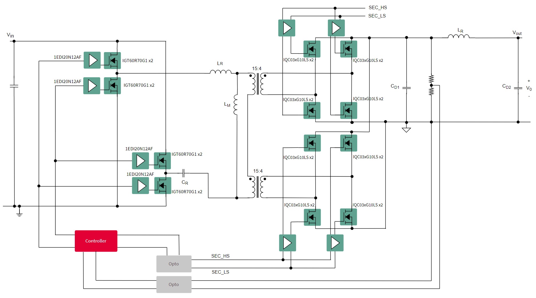 Figure 3: A 3.6 kW DC/DC LLC full bridge to full bridge design with two transformers in series in the primary side and in parallel on the secondary side for forced-load sharing.
An EiceDRIVER series dedicated to GaN HEMT is available that ensures optimal control. These deliver the continuous gate current, lying at a few mA, required to maintain the “on” state. Due to the fast switching transients and inherently low threshold voltages, they can also deliver a negative “off” voltage that is duty-cycle independent.
Taking the same approach with a 3.6kW, 385 to 52V DC/DC LLC delivers even higher efficiency improvements when switching to CoolGaN, says Infineon. Although the silicon MOSFET and GaN transistors used exhibit similar RDS(on) values, the CoolGaN implementation has a peak efficiency of 97.83% in this 160W/inch3 design. This results in a 15% reduction in heat dissipation over the silicon-based design.
Using a CoolGaN-based totem-pole PFC, efficiency can be improved with the addition of CoolGaN in the two full bridges of the secondary synchronous rectifier stage that offer optimal sharing of the load (Figure 3). When subtracting the impact of the cooling fan and the internal housekeeping supply, the GaN-based design attains a peak efficiency of almost 98.5%.
Innovation in semiconductor technology alone does not deliver at the application level. Miniature surface-mountable packaging exhibiting low inductance leakage simplify designs, especially at the high switching frequencies being used. PG-VSON, measuring just 5.0 x 3.0 x 1.075mm, helps keep traces short. Its construction is also suited to passive heat dissipation and low-profile or narrow rack- or wall-mounted solutions (Figure 4).
GaN for 5G
GaN is often thought of as an essential component in enabling 5G RF transceivers, but it is clear that it is so much more. The practicalities of exchanging existing 4G BTS hardware for 5G and sourcing and renting new locations for AAS and small cell BTS mean that size, volume, and weight require as much consideration as the functional requirements.
 Figure 4: The PG-VSON surface mount package with low inductance leakage by Infineon.
Infineon’s portfolio of CoolGaN HEMT transistors, coupled with appropriate EiceDRIVERs, ensure that power converter efficiencies can be improved across the desired load range. This enables the required reductions in weight and volume through innovative heat dissipation and construction approaches, while also ensuring robustness and reliability to keep maintenance and downtime to a minimum.