


In the world of EV charging, efficiency is a prime concern. This is not just to get more range as quickly as possible, but also to reduce cost to the supplier – you only pay for what you get, not for what’s lost as heat, which also has an environmental impact, which should be minimised. Higher efficiency also means a smaller, lighter, and cheaper charger, all things being equal, and that can be a real commercial edge.
The outline of a charger is always similar – AC mains, whether single- or three-phase, is converted into a constant DC which is then further converted, usually with isolation, to a controlled current to charge the battery. It is a statutory requirement that the charger takes AC current as if it were a resistive load, that is, the current waveform should match the voltage waveform, nominally sinusoidal. Passive rectifying ‘front ends’ tend to make distorted current waveforms, so this must be addressed. PFC or ‘Power Factor Correction’ is the traditional term for the correcting function, but ‘harmonic reduction’ also applies, as it’s possible to have a high-power factor but with a distorted waveform producing current harmonics that utilities object to. International standards define the allowable limits of harmonics in power – IEC 61000-3-2 up to 16A and IEC 61000-3-4 over 16A.
There are multiple choices for a ‘front end rectifier’
‘Active Front End’ is the term for the combined function of rectification, current harmonics reduction and regulation of the resulting DC. As efficiency must be high, a multitude of design approaches have been developed as being optimum for single- or three-phase inputs under different conditions and cost constraints. The simplest approach is to bridge-rectify AC then boost it to a DC voltage higher than the peak of the AC, with voltage and current sensing to simultaneously regulate the DC voltage and force the input current to follow the same shape as the nominally sinusoidal input AC voltage. The outline is shown in Figure 1 (left) as a ‘modular’ approach for a three-phase supply. The three DC outputs are separately converted and connect to one or more isolated DC-DC converters (not shown) that control power flow to the batteries. The bridge rectifiers however introduce unacceptable losses, with a total of six diodes conducting at any point of a three-phase mains cycle. The ‘Totem Pole PFC’ (TTPFC) version replaces diodes with semiconductor switches for lower conduction loss, although the topology had to wait for wide band-gap semiconductors before switching losses became acceptable, when operating in continuous conduction mode, necessary at high power. Figure 1 (right) shows three TTPFC stages used in a three phase ‘Y’ system. The TTPFC also has the benefit of possible bi-directional operation when controlled appropriately.
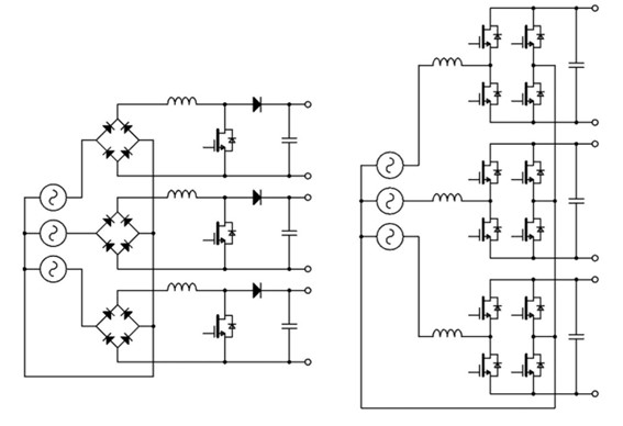
Figure 1: The basic ‘modular’ three-phase boost PFC stage left, and the totem-pole PFC, right
In three-phase systems, a modular approach can continue to operate if a phase fails. In this situation however, the rectifier would be required to shut down anyway. Also, the number of interconnections is a disadvantage. Circuits with line frequency inductors can be simple, but size, weight, distortion, and cost effectively prohibit their use. A single boost switch after a diode bridge with a high frequency inductor in each phase as in Figure 2 (left) is much smaller overall than the modular approach. This can be simplified to use a single inductor as in Figure 2 (right). However, in both cases the total harmonic distortion (THD) is unacceptable, reaching 30%. Typically, a THD figure of 5% or less is required in industrial and EV charging systems.
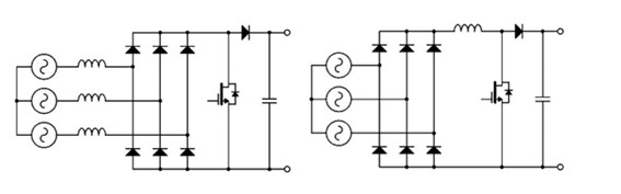
Figure 2: Boost PFC with three line inductors left, and alternatively, right, a single inductor after three-phase rectification
Current injection shapes input current
The solution to the high distortion is to inject a suitable current into the phase such that sinusoidal current draw is forced. Two series switches are needed for each phase, as current injection must be facilitated in both polarities depending on the point in the AC cycle. The outline circuit shown in Figure 3 (left) is a popular variation of the ‘Vienna Rectifier’ invented in 1993 by Johann W.Kolar [1]. The circuit has the advantage that the switches only block half of the DC output voltage, so 650V devices can safely be used in 480VAC line-to-line systems. The Vienna rectifier shown is uni-directional but can be made bi-directional as in Figure 3 (right) by replacing the diodes with 1200V-rated switches, which also give a useful reduction in conduction loss. The circuit is identified as the Three-Level Transistor Neutral Point Clamped topology (3L-TNPC).
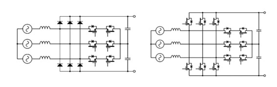
Figure 3: The Vienna rectifier left, and Three Level TNPC right
Both of these topologies are three-level types with reduced component stress and low ripple in the inductors. If three-level control complexity is seen as problematic, then the circuit could be simplified further to the common Two-Level Voltage Source Inverter arrangement (2L-VSI), although the switches now need to be rated at the full DC output voltage and the inductors must be larger for a given switching frequency, imposing twice the volt-seconds upon the inductors. This reduces complexity but still allows full current shaping. Compared with the Vienna rectifier and 3L-TNPC circuits, losses are typically higher however, especially at light loads.
Efficiencies compared
In all of the topologies, the gate drives are pulse width modulated to regulate the DC output and force sinusoidal current draw. PWM can be implemented in different schemes such as the basic ‘sine-triangle’ method, or in more complex ways such as ‘space vector’ (SVM) or ‘discontinuous modulation’ (DPWM1), the latter achieving lower switching losses due to clamping to a DC link rail during a 60° interval twice during each line cycle.
To compare the performance of the different topologies and modulation schemes, company UnitedSiC used their online FET-Jet Calculator [2] to compute efficiency under common conditions (Tables 1 and 2).
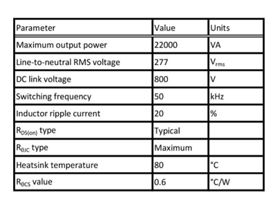
Table 1: Reference conditions for comparison of Active Front End topologies
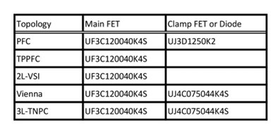
Table 2: Semiconductors selected
The semiconductors selected are economical solutions and it would of course be possible to improve any one efficiency result by selecting different devices but with added cost. The calculator results are shown in Figure 4.
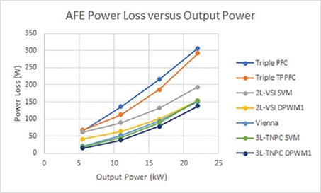
Figure 4: Power loss comparisons between topologies and modulation schemes
As expected, the ‘modular’ triple PFC and TPPFC approaches have highest losses with multiple semiconductors in the power paths. The 2L-VSI topology with fewer in-line switches is next best with space vector modulation (with almost identical loss as sine-triangle modulation), and with DPWM1 modulation it can rival the Vienna rectifier, at least at higher power levels. The 3L-TNPC with SVM offers further marginal improvement, but with DPWM1 modulation scheme, losses are lower still.
Conclusion
The analysis using UnitedSiC’s calculator shows a range of efficiencies attainable in an active front end from 98.6% to 99.3% for the power semiconductors. These might both seem creditably high figures, but the in terms of losses represent more than halving, from worst to best. This has a direct impact on the size, weight and cost of cooling, or alternatively lower losses can yield lower junction temperatures and higher reliability. These factors, along with device and energy costs, and complexity of gate drives and controllers all have to be weighed against each other to define an optimal solution for any particular application.
References
[1] J. W. Kolar, „Dreiphasen-Dreipunkt-Pulsgleichrichter“, filed Dec. 23, 1993, File No.: AT2612/93, European Patent Appl.: EP 94 120 245.9-1242 entitled “Vorrichtung und Verfahren zur Umformung von Drehstrom in Gleichstrom”.
[2] https://info.unitedsic.com/fet-jet