


PC manufacturers were then using MOSFETs housed in SO8 packages as power switches for computing devices’ microprocessors. The SO8 package has no copper pad exposed on the underside, thus limiting its ability to dissipate heat. It also uses thin bond wires to connect the die source terminal pins, extended outside the package. Since the package uses very thin wire diameters, the ohmic resistance is relatively high, resulting in inefficient performance.
In the 90s, this wasn’t a significant problem because the limits of semiconductor processing technology meant that the resistance of the silicon die was the main contributor to the overall RDSON of a MOSFET. But as the transistor count and operating frequency of microprocessors continued to scale, their current demand also rose while the required supply voltage reduced to below 1 V. So, the MOSFET power switches were required to switch peak currents of up to 120 A, 190 A, and more. At these current levels, the SO8 package lacked the necessary thermal performance to dissipate the heat resulting from internal I2R losses. So, the industry switched to DPAK, which has a copper plate on the underside to promote heat transfer from the package into the PCB. However, the DPAK has a much larger footprint than SO8. As microprocessors got even bigger and faster, they required larger, multiphase power supplies to meet the demand for operating current, making it necessary to connect several MOSFET switches in parallel. Hence demand grew for a package significantly smaller than DPAK yet with great thermal performance.
This desire to deliver more power while maintaining a compact power supply footprint inspired the next generation of MOSFET packages, which combined the popular SO8 footprint with an exposed copper pad like the DPAK. However, the standard SO8’s internal bond wires then became the dominant factor limiting thermal performance. Further internal changes were needed to raise the performance to compare with the larger package. Replacing the bond wires with a large copper clip attached to the source metallisation on the topside of the die significantly lowered both the die-to-ambient thermal resistance and the device’s overall electrical on-resistance (RDS(on)).
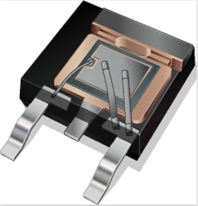
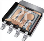
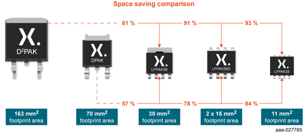
And so, in 2002, the ‘loss-free package’ was born with the introduction of 25 V MOSFETs in LFPAK56 (named after its dimensions – 5mm x 6mm). Having four pins on one side – like the SO8 – and a single large tab on the opposing side, these had RDS(on) and maximum drain current comparable to those of similar devices already on the market in the larger DPAK. Despite having a 30mm2 footprint, which is less than half that of the DPAK’s 70mm2, the thermal performance of LFPAK MOSFETs is as good as DPAK devices.
Changing industry perceptions
Surprisingly, instead of immediately rushing to welcome this innovation, the market’s initial reaction was, “How can this package have the same thermal performance as one twice its size?” There was also skepticism about the reliability of the clip attachment, which is soldered to the source connection. In fact, the copper clip improves reliability by eliminating areas of high current density and temperature ‘hotspots’ at the locations where bond wires are attached.
The results from reliability and thermal performance testing demonstrated that the LFPAK could perform as claimed. The real clincher came when LFPAK56 was awarded the AEC-Q101-Rev D qualification required for use in automotive applications. Meeting the exacting standards set by this industry provided massive reassurance about its use in other applications.
Needless to say, the LFPAK56 became hugely popular among manufacturers providing subsystems to automotive OEMs by allowing them to save the board space previously occupied by larger DPAK devices. In the most recent testing for AEC-Q101-Rev D qualification, LFPAK exceeded the requirements for all tests; in fact, surpassing the Highly Accelerated Stress Test (HAST) specification by a factor of 17. For some tests, it was almost impossible to induce a single device failure, due to the test PCBs failing before the devices under test!
With ongoing advances in semiconductor process technologies, the die-free package resistance has become a more significant factor determining the overall device RDS(on). This has further increased the popularity of LFPAK, as its low ohmic resistance lets manufacturers exploit the superior performance of the latest silicon.
LFPAK today
The LFPAK88, measuring 8mm x 8mm, and the 3mm x 3mm LFPAK33 soon followed the LFPAK56, making the electrical and thermal performance advantages of the latest package technology available for devices in a wide range of voltage and current ratings.

Today a single MOSFET in LFPAK88 can have RDSON of just 0.55 mΩ and can handle a maximum current of 500 A. In addition, dual LFPAK devices containing two individual MOSFET dies in one package deliver an extra space-saving option for designers. This is proving extremely popular, especially in automotive applications.
And it’s not only MOSFETs. Many bipolar power transistors, of course, are also offered in LFPAK, Among other standard power packages. Overall, LFPAK has been hugely successful; Nexperia shipped more than 1.7 billion devices in 2021 and around 90% of the product range is now LFPAK-based.
The future for LFPAK
The industry is constantly looking to bring the benefits of using low RDSON power MOSFETs to new applications. For example, automotive OEMs needed an electronic solution to replace conventional battery-isolation fuses that disconnect the battery in the event of a short circuit to protect the vehicle’s electrical systems. The fuse is a one-shot component, obviously, and must be physically replaced either at the roadside or at a service location, which is inconvenient and expensive. The high current-handling capability of a copper-clip package allows building automatically resettable e-fuses rated for 400-600 A continuous current in normal operation, and surge current over 1000 A, using a relatively small number of MOSFETs. A suitable fuse module could contain, say, four or five MOSFETs in LFPAK88, or a pair in CCPAK1212, which is a new package style that leverages the copper-clip knowhow developed for LFPAK. Moreover, the e-fuse can be controlled to limit the inrush current supplied to demanding loads, allowing the wiring loom to be made thinner and lighter to benefit economy and driving range.
The high thermal performance, energy efficiency, and current rating of LFPAK MOSFETs also makes them an ideal choice for some emerging motor-driven applications such as active suspension systems that are used to improve driver comfort and are also used as safety systems to minimise the impact of collisions on the occupants in the vehicle. In addition, LFPAK MOSFETS are extending battery life in cordless power tools and garden equipment and were recently used in a novel powered surfboard to enable surfing without waves. Who knows where else they might be found in years to come!