 still relevant?")
Is the MOSFET figure of merit (FoM) still relevant?
As gate drivers are now capable of efficiently meeting large Qg requirements and faster switching topologies create smaller, more efficient systems, some often ignored parameters have now become system-critical.
We are accustomed to looking at the figure of merit (FoM) for MOSFETs as a product of RDS(on) and gate charge (Qg). But is the traditional FoM definition still relevant?
From a conduction and switching performance perspective we are all accustomed to looking at the FoM for MOSFETs as a product of the drain-source on resistance RDS(on) and the gate charge Qg (FOM = RDS(on) x Qg).
It was a good indicator at the time of its definition, but most modern MOSFETs now have an optimised Qg. In pursuing the traditional FOM some manufacturers are spending resources to further optimise an already good Qg at the potential expense of other critical parameters.
The traditional FoM definition often acts as a gating factor for MOSFET selection, for today’s motor drive and switch mode power supply (SMPS) topologies. We therefore need to elaborate on how important Qrr is and how Qg is becoming less critical. Redefining the MOSFET’s FoM would allow the choice of the right MOSFETs to improve efficiency but also bearing in mind voltage spiking and the design’s EMI signature.
The role of Qg
Qg in its purest sense, helps define the switching times at any given gate drive current and gives a practical comparison of switching performance between MOSFETs. For example, theoretically a MOSFET with 50nC being driven by a 1.0A source and sink current, can be turned on in 50ns and turned off in another 50ns. A MOSFET with a lower Qg can therefore be turned on and off quicker for any given gate drive current, potentially reducing switching losses.
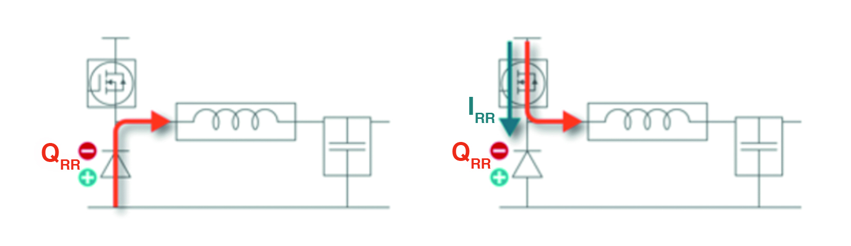 Figure 1: Qrr and shoot through in synchronous buck topology
It is not quite that simple. A 50nC MOSFET switching a 48V line and a 5.0A drive can be turned off in 10ns, but it will result in an enormous 48,000V/µs of dv/dt. This is why almost every application uses an external gate resistor (Rg) to control dv/dt and its associated effects. Adjusting Rg during the design-in stage has a great impact in achieving the required switching performance.
In older systems, the gate driving capacity of controllers was a limiting factor, especially in applications where the MOSFETs are paralleled. The gate driving capacity of today’s controllers has increased significantly, however and in more complex topologies a simple external gate drive stage can easily provide sufficient source and sink currents to drive several hundreds of nC under most practical conditions.
Even in terms of power efficiency, from an overall system perspective the losses when charging and discharging a gate are usually only a small fraction of the system power rating. That makes them effectively negligible for most applications. In practical terms, even a considerable Qg difference can have a minimal or even no effect on most applications. However, it is worth noting that this power is dissipated in the gate drive components (external Rg and gate driver) so appropriate thermal provisions need to be made (Table 1).
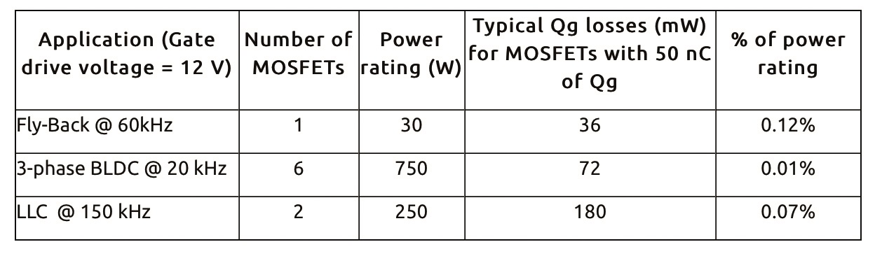 Table 1: Losses in real-life applications
Qrr in switching applications
When the body diode of the MOSFET is allowed to conduct, e.g. in synchronous rectification applications (Figure 1) and during the continuous conduction mode of operation, the effects of Qrr are evident.
During dead time, both high side and low side FETs are turned off allowing the low side body diode to conduct the freewheeling current. This results in stored charge (Qrr) which is removed in the form a momentary shoot-through when the high side FET turns on. The turn on speed of the high side FET, sets the di/dt of this recovery current. Recovery losses together with this recovery current, in combination with the circuit’s parasitic elements can result in a voltage spikes (Figure 2).
During stage five of a full-bridge conversion, the body diode of Q2 is reverse biased while it is still conducting current. This results in a recovery current that flows through Q1 and the body diode of Q2, which represents a shoot-through scenario until the body diode of Q2 is completely recovered. After the recovery instant, the parasitic inductance in the current path results in a voltage swing to try to maintain the current in the path. This voltage excursion coupled with the parasitic elements in the path results in ringing at the switch node, leading to EMI.
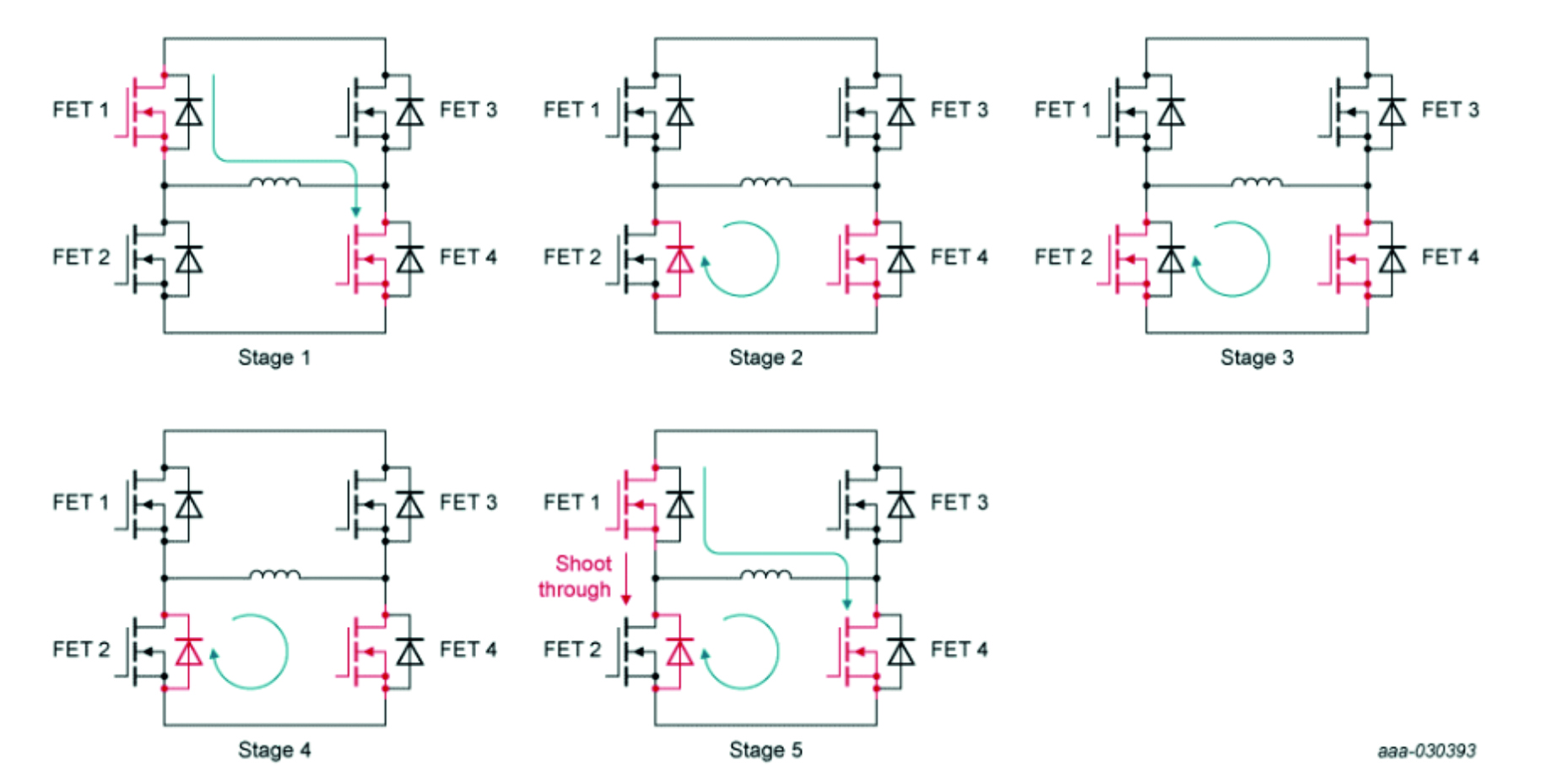
Figure 2: Qrr and shoot through in BLDC full-bridge topology
The effects of Qrr in flyback and other SMPS topologies, especially operating in continuous conduction mode are profound. Consider a flyback topology when the primary side MOSFET is off. Energy is transferred from the primary to secondary side, yet just before the primary side is turned on at the start of the next cycle, the synchronous controller turns off the MOSFET to prevent a shoot-through allowing the body diode to conduct for the remaining time period. When the primary side turns on at the beginning of the next cycle, the secondary MOSFET conducts in the reverse direction until the store charge is recovered, resulting in a momentary shoot-through.
A new MOSFET FoM
Qrr-related shoot-through is a major source of failure in SMPS. In addition, Qrr-related voltage spiking and dv/dt make snubber design complex and lossy and also results in an unwanted EMI signature.
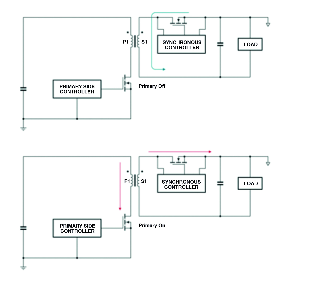 Figure 3: Qrr and shoot-through in flyback and other SMPS topologies
The widespread nature of the effects of the Qrr means it is critical for efficiency and an important parameter for ease of design and system reliability.
Given the undeniable impact the Qrr parameter has across the spectrum of switching applications, it is strongly recommended to include it into the equation when selecting a MOSFET. At the same time, given the impact Qrr has on the overall health of the system, compared to the Qg, the Qrr switching parameter cannot be ignored.
Siva Uppuluri is international product and marketing manager for Nexperia
Product Spotlight
APV1111GVY
Panasonic

Panasonic PhotoMOS® Photovoltaic MOSFET High-Power Drivers
| SKU: | |
|---|---|
| Stock: | 3490 |
| Cost: | $3.95 |
