


This article originally appeared in the May’23 magazine issue of Electronic Specifier Design – see ES’s Magazine Archives for more featured publications.
Power conversion products have certainly benefited from the introduction of wide band-gap semiconductor switches such as SiC FETs – a normally-off cascode combination of a SiC JFET and silicon MOSFET. The devices are capable of ultra-fast switching with low conduction losses, showing gains in efficiency and power density in a wide variety of applications. However, the high voltage and current edge rates interact with board parasitic capacitances and inductances to a greater extent than with older, slower technologies, which can result in unwanted induced currents and voltages, reducing efficiency, stressing components and impacting reliability. Further, with SiC FET on-resistance now typically measured in milliohms, PCB track resistances can be comparable and must be carefully minimised to maintain low system conduction losses.
Putting a scale to current edge rates
Current edge rates of over 1000A/µs are easily possible with SiC FETs (Figure 1) and this produces voltage transients from inductance around the switching loop between the SiC FET, its load and local decoupling capacitors (Figure 2). For example, according to E = -Ldi/dt, 100nH loop inductance generates a transient of 100V which adds to the device operating voltage, reducing margin to breakdown and increasing EMI.
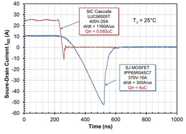
Figure 1: SiC FET switching waveform showing >1000A/µs edge rate compared with a Si SJ MOSFET of the same class
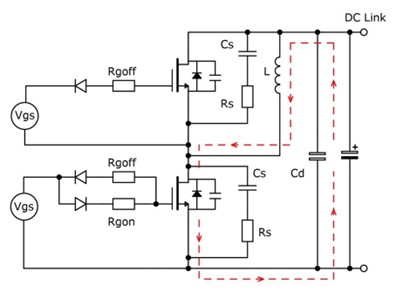
Figure 2: A typical switching loop experiencing high di/dt
This inductance value is realistic – in a typical power application, components cannot be tightly packed due to their physical size. For example, just 50mm (l) of PCB track for each of a ‘go’ and ‘return’ connection has a total of about 100nH inductance for 2.5mm width (W) and 2oz (0.07mm) copper weight (T), calculated from Equation 1, from Terman.
![]()
This relationship is for isolated go and return tracks, not a single track above a return plane. It is interesting to see that when plotted, there is relatively little dependency of inductance on track width and even less on thickness, length being the major factor. Figure 3.
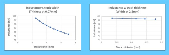
Figure 3: Variation of isolated track inductance with thickness and width according to Equation 1
The plots show that maximum benefit can be realised by reducing length, which can be effectively achieved by placing high-frequency decoupling capacitors, Cd in Figure 2, closer to the switches than the bulk DC-link capacitors, especially if these are not low inductance types. If the go and return paths are close, typically using a copper plane, then inductance is dramatically reduced (Figure 4).
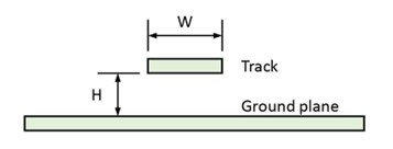 Figure 4: A return plane below a track strongly reduces total inductance
Using Equation 2 from Clayton [2], our 2.5mm (W) track separated from a return plane by 1.6mm (H) now has a total loop inductance of only 32nH. The equation is valid for W/H>1 and again, track thickness is not a major contributor, but track width now has a strong influence as does distance between track and plane (Figure 5). If return planes are placed both above and below the track, inductance reduces further still, with the added advantage of more screening.
![]()
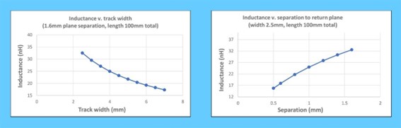
Figure 5: When the return path is a copper plane, inductance reduces and varies strongly with separation and track width
As well as tracks, vias add some inductance and should be avoided anyway in the power path if possible, because of their resistive voltage drop. The inductance of a via depends on dimensions and whether it is filled or not, but is approximately 0.5nH unfilled for 0.5mm diameter and 1.6mm length. This value can typically be ignored, especially if several are paralleled, which might be the case in a power path.
Common connection inductance in gate and source connections is problematic
If the SiC FET gate drive loop and its source current share any length of tracking, the inductance of the common connection causes a voltage transient with a load current step which acts against the gate drive (Figure 6). In the worst case, an off-drive signal is reduced in amplitude which could result in ‘phantom turn-on’ causing ‘shoot through’ in a bridge converter leg, with potentially catastrophic damage. Even with a separated gate drive return to the source of a three-lead TO-247 device there is still about 10nH of package inductance which is common and cannot be eliminated, producing a transient of ten volts with 1000A/µs source current edge rate. These edge rates are often slowed in practical designs, but a solution anyway is to use four-lead devices with a separate internal ‘Kelvin’ connection to the source, such as are available from UnitedSiC (Qorvo) [3]. This reduces common connection inductance to the die figure of around 1nH, allowing faster edge rates and potentially lower dynamic losses.
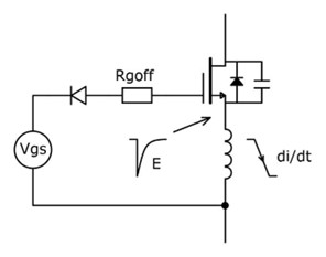 Figure 6: A gate voltage transient results from high source di/dt and common connection inductance
Circuit capacitances can cause unwanted coupling
Having noted that wider tracks usefully reduce inductance and voltage transients, unfortunately they also increase capacitance to adjacent tracks, components and ground. With the high dV/dt rates seen with SiC FETs, displacement currents are induced, which can cause high EMI levels and chaotic operation. For example, SiC FETs can easily switch at 100kV/µs edge rates which would induce 1A through just 10pF. The current flows around a system with a route that would normally be difficult to identify. A particular problem is capacitance to the main switching node at the source connection of a high-side switch. This could be physically isolated to avoid coupling to any sensitive control or feedback connections. However, there is always a path through the gate driver to the rest of the system and even if this is isolated magnetically or through an optocoupler, there will be residual capacitance through the signal path and through any DC-DC converter providing gate drive power. For this reason, care should be taken to specify isolating parts with low coupling capacitance, ideally no more than a few pF.
A major source of common mode EMI which could cause statutory limits to be exceeded is capacitance between switching nodes and chassis ground. Fortunately, the efficiency of devices such as SiC FETs often means that they can operate with small ungrounded heatsinks. If a larger grounded heatsink must be used, an electrostatic screen in the form of copper foil can be used between the switching device and heatsink, although this inevitably worsens thermal resistance and must be carefully insulated to meet safety standards.
Thermal considerations
Often with SiC FETs, their losses are so low that PCB tracks and planes can be sufficient heatsinks to keep junction temperatures within reasonable limits. Quantifying thermal resistance of such arrangements can be difficult, due to interaction with other heat-generating components, so multiphysics simulation software is often used to predict results. The PCB material, number of layers and their copper weight, airflow direction and rate, surface emissivity and cross heating from other components must all be factored in.
Heat can be transferred through a PCB using thermal vias, improving on FR4 with its core thermal conductivity of only about 0.25W/m-K. A via 0.5mm diameter, 1.6mm long, unfilled with a wall thickness of 0.025mm has a thermal resistance of about 100°C/W (Figure 7).
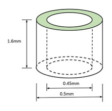
Figure 7: A typical via has a thermal resistance of about 100°C/W. Resistance is about 0.7 milliohms and inductance is about 0.5nH
As an example, just 12 thermal vias of this dimension would halve the thermal resistance of a 25mm square PCB area 1.6mm thick from a copper plane on the top to copper on the bottom from about 16°C/W to around 8°C/W. An insulated metal substrate (IMS) has about 45% of the thermal resistance of FR4 but has the disadvantage of higher cost and a practical limit to the number of layers. IMS dielectric thickness is usually around 0.15mm per layer for minimum thermal resistance, which is usually the goal, but this does result in relatively high capacitance, with the resulting possibility of high common mode currents as discussed. IMS substrates are typically used in high-density applications for maximum heat extraction to a plate with liquid or forced air cooling. For less critical systems with convection cooling, FR4 with thermal vias to copper planes might be more suitable. With switching devices increasingly available with top-side cooling, less reliance is placed on the thermal path through the PCB.
UnitedSiC (Quorvo) has shown that a simple RC snubber can be an overall effective way to limit over-voltage transients at switching edges, compared for example, to slowing the gate drive with series resistors. Relatively small surface-mount components can be used with little dissipation for a useful reduction in peak voltage. The snubber should be placed as close as possible to the device with tracks of sufficient width to minimise inductance and to dissipate the power necessary. A thermal break in the track in the form of a short ‘neck’ might help to reduce cross heating from the power device.
PCB tracking resistance reduces efficiency
SiC FETs are now available with on-resistances of just a few milliohms, even at high rated voltages, so their conduction loss can be very low. However, associated track resistance can become comparable and should therefore be minimised to maintain the SiC FET advantages. To evaluate the effect, PCB resistance depends on copper resistivity, thickness, temperature and track length. A convenient measure is the number of ‘squares’ along the track, for example, 35µm/1oz copper has 0.5 milliohms resistance per ‘square’ in any dimension at 25°C, so a 1mm wide track 1mm long has the same 0.5 milliohm resistance as a 10 mil wide track 10 mil long. For 2.5mm tracks therefore, just 100mm length, as used in our inductance calculations, would measure 20 milliohms – typically much more than the lowest SiC FET on-resistance. Also, at higher temperatures, copper resistance increases, to about 26 milliohms at 100°C in this example, so this should be factored-in. The ‘counting squares’ method is accurate for straight tracks – if there are abrupt turns, for example, the resistivity at the corner increases due to current crowding effects. Sharp corners should anyway be avoided to prevent localised high electric field intensity and increased risk of voltage breakdown.
With AC, the ‘skin effect’ should be taken into consideration, where, as frequency increases, current tends to increasingly flow on the surface rather than in the bulk of a conductor. However, the effect is typically small with PCB tracking; skin depth is approximated by 66/f1/2 mm so even at say, 1MHz, switching current flows to 0.07mm depth or the total thickness of 2oz copper. Harmonic currents would not penetrate so deeply but their amplitude is anyway lower.
When high frequency AC returns through a copper plane, it might be assumed that the resistance is lower in this path. However, the benefit is not substantial as current concentrates immediately below the power track and only DC components spread out significantly (Figure 8).
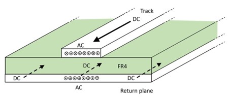
Figure 8: AC return current in a plane concentrates below a power track. Any DC component present spreads wider
Conclusion
Real-world connection resistances should be understood and reduced to maximise the potential performance of SiC FETs. Parasitic inductance and capacitance generally should also be reduced although these could form part of resonant tanks in some conversion topologies. In this case it is still important to quantify and control the circuit values.