








Hardware startups and small teams usually start out with standalone printed circuit board design tools. This setup works fine when a company has only a small number of engineers working together in the same room; they pass files around, manage bills of materials in spreadsheets, and manually check component availability.
But global supply chains are messy and, perhaps most importantly, distant. Parts go out of stock, and lead times fluctuate wildly. A 2024 Protolabs survey shows that most organisations are developing new products faster to stay competitive, leaving little buffer for manual data entry or miscommunication.
When product complexity grows, the old workflow breaks down. An engineer might design a board, wait two weeks for a design review, and by the time procurement places the order, a critical microcontroller is no longer available. A single missed email or a local file overwrite can, and often does, result in the factory making the wrong board revision.
Key takeaways
- Teams usually outgrow standalone tools when engineers spend more time managing data and procurement than actually designing
- Mid-sized teams need managed workflows and part-library governance to scale without taking on heavy IT setups
- Enterprise organisations require deep digital thread integration, regulatory compliance tracking, and strict access controls
The tipping point: signals you need an enterprise platform
You know a team has outgrown its PCB tool when the time spent on actual engineering work drops. Industry research shows that engineers at traditional firms often spend barely half of their working hours on active design tasks. Much of the rest goes to administrative work (75%), tracking down components, and fixing errors caused by disconnected tools. In fact, Fictiv’s 2026 Manufacturing and Supply Chain Report found that 83% of engineers spend, per week, four hours or more on procurement-related tasks.
Standalone tools rely heavily on human effort for coordination. You might notice your team struggling with version control, dealing with outdated component libraries, or spending hours formatting BOMs for procurement. When multiple designers try to edit the same board in a standalone environment, conflicts and rework almost always happen.
Essentially, everybody is working in functional silos, whether that be electrical engineers in their ECAD tools, mechanical teams using MCAD, or sourcing taking place in spreadsheets. These tools served their purpose before, but they just cannot handle the data load of a modern supply chain.
The solution? An enterprise PCB design platform.
What capabilities separate an enterprise PCB design platform from a professional standalone tool?
An enterprise PCB design platform moves a team from file-based handoffs to a shared digital workspace. It brings all disciplines into the same continuous workflow.
Here are the specific capabilities that separate them:
- Process control: enterprise platforms enforce configurable workflows for design reviews, part requests, and project creation
- Data access and security: enterprise solutions provide single sign-on (SSO), advanced user data permissions, and enterprise-level event monitoring and logs to track who did what
- Traceability for compliance: an enterprise system tracks every single change and decision to create a transparent audit trail
- Deeper integration: while standalone tools might offer basic connectors, enterprise platforms integrate deeply with PLM and ERP systems to sync BOM data continuously
In practice, instead of an engineer exporting a manual spreadsheet and emailing it to a purchasing manager, the platform syncs the data natively. This means procurement sees live part availability while the engineer is still routing the board.
What is the difference between Altium Designer, Cadence Allegro, and Siemens Xpedition for professional PCB design?
These three tools are the heavyweights in professional PCB design.
On one hand, you have Cadence Allegro and Siemens Xpedition, both of which historically provided top-of-the-line layout and routing features for cutting-edge digital systems. Altium Designer has steadily surpassed those routing capabilities while also improving and modernising the user interface, directly addressing many of the common criticisms of Cadence’s and Xpedition’s legacy software interface.
Even as Altium’s layout and routing features became more advanced, the software became part of a larger platform dedicated to serving the entire product development process. By connecting the Altium Designer desktop tool to the Altium 365 Cloud platform, the company created a shared space for different engineering disciplines. This approach gives hardware teams a way to manage data and workflows without bolting on 3rd party solutions or using outdated vendor-specific solutions.
What is the best PCB design tool for mid-sized hardware teams?
The best tool for a mid-sized team balances structure with speed. These teams face growth and organisational needs, like managing supply chain risks and cross-domain collaboration, but they lack dedicated IT departments to manage complex servers.
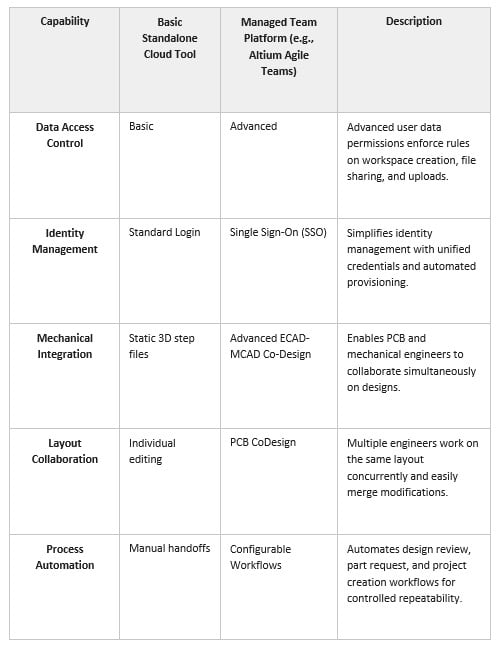
A practical approach is to use a turnkey platform. As an example, platforms like Altium Agile Teams handle this by offering out-of-the-box Cloud workspaces with no complicated setup or implementation required. With platforms like Altium, instead of managing local server permissions, engineering managers can easily bring internal PCB designers and external project collaborators into a shared Cloud environment. Multiple team members can even co-author the same PCB layout at the same time.
Here is a breakdown of how it compares to a professional standalone-plus-Cloud setup:
What is the best PCB design software for enterprise companies?
Enterprise organisations have many users contributing to complex projects, but they need a platform that helps keep project data synchronised while documenting changes, core functional requirements, and tracking each data release to manufacturing. After all, they operate in highly regulated industries like automotive, medical, and aerospace. They must build compliance into every single stage of development, from design decisions to component selection and audits.
Platforms built for this tier focus heavily on connecting users, controlling data access, and security, and enabling collaboration while also tracking requirements, project revisions, and manufacturing releases. For example, solutions like Altium Agile Enterprise natively integrate this ECAD data directly into PLM, ERP, and 3rd party data management tools. For companies building in highly regulated industries, documentation across revisions aids broader compliance efforts, for example, in medical device development.
Which PCB design tool scales best for enterprise?
The answer should be clear: a fully-featured PCB layout tool that easily integrates into a Cloud platform for data management and multidisciplinary collaboration is the best option for scaling from a small team to a large enterprise. A single vendor offering the entire solution suite, like Altium, allows a team to grow and seamlessly transfer their data into a cloud environment, resulting in zero project data loss and requiring no file conversions. All Cloud tools should be accessible on day one and have no impact on the day-to-day design and layout tasks that engineers must perform.
By integrating supply chain data, a portal for MCAD collaboration, and automated data tracking and release processes, teams can work across traditional boundaries and focus on developing entire products, not just printed circuit boards. In addition, building on a Cloud platform gives users access to additional solutions, such as GovCloud for ITAR compliance, or an option to deploy on-premises behind a VPN for even greater control over data access and security.
Frequently asked questions
How does real-time BOM management help engineering teams?
Real-time BOM management continuously syncs data across teams to reduce late-stage surprises. Industry benchmarks show that fixing an error in manufacturing costs up to 10 times more than fixing it in the design phase, making real-time visibility critical. It allows engineers and procurement to co-design BOMs and see the impact of component availability on design decisions immediately.
Can external contractors securely access an enterprise PCB platform?
Yes. Modern platforms use role-based team permissions and guest collaborator access. This ensures external partners only see the data they need, protecting the company’s intellectual property.
Does adopting an enterprise system slow down design speed?
If configured correctly, no. A platform like Altium Agile automates repetitive workflows like design reviews and part requests. This structured repeatability reduces human error and actually frees up time for engineering work.
What is the next step to move away from my current standalone tool?
You should evaluate your specific needs based on your team size and regulatory requirements. Do you just need better library governance, or do you need full PLM integration? Answering that will dictate the exact edition you require.