


This method redistributes integrated circuits (ICs) on a wafer, providing more space for electrical connections, thereby improving thermal performance, reducing the form factor, and increasing overall efficiency.
FOWLP is essential for producing high-performance, compact electronics used in smartphones, household appliances, and automotive systems.
History and evolution of FOWLP
The concept of FOWLP emerged in the early 2000s as a solution to the limitations of traditional wafer level packaging (WLP). Early WLP methods involved packaging ICs directly on the wafer, which restricted the available space for interconnections and limited performance. FOWLP addressed these issues by redistributing the ICs on a larger area, providing more space for connections and enabling higher performance. Over the years, advancements in materials and processes have further refined FOWLP, making it a standard in high-performance semiconductor packaging.
The advantages of FOWLP
FOWLP offers several advantages over traditional semiconductor packaging methods. By expanding the space available for electrical connections, it allows for better thermal management and improved electrical performance. This makes it ideal for industries that demand high-performance, compact devices. Electronics manufacturers, particularly those producing smartphones, tablets, and other consumer electronics, benefit significantly from FOWLP. The automotive and industrial sectors also leverage this technology to enhance the performance and reliability of their electronic systems.
By providing more space for electrical connections and improving thermal management, FOWLP addresses the limitations of traditional packaging methods.
How FOWLP is created
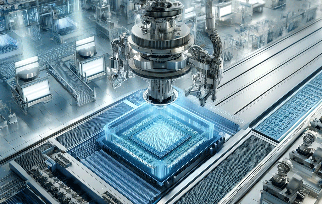
The FOWLP process begins with dicing the wafer into individual chips. These chips are then reconstituted on a carrier wafer using a moulding compound. Redistribution layers (RDLs) are applied to create interconnections between the chips. The final step involves creating bumps or solder balls on the RDLs, enabling the IC to be mounted onto a printed circuit board (PCB). This approach improves thermal performance and efficiency by allowing more effective heat dissipation and reducing electrical resistance.
What is next for FOWLP
The future of FOWLP looks promising as the demand for high-performance, compact electronic devices continues to grow. Researchers and manufacturers are exploring new materials and techniques to further enhance the capabilities of FOWLP. Innovations in three-dimensional (3D) packaging, heterogeneous integration, and advanced RDL technologies are expected to drive the next wave of improvements in FOWLP. As these advancements unfold, FOWLP will play a crucial role in meeting the evolving needs of the electronics industry.
With a history rooted in the early 2000s, FOWLP has evolved to become a key technology in the electronics industry. Looking ahead, continued innovations promise to further expand the capabilities and applications of FOWLP, solidifying its importance in the future of semiconductor packaging.