


Advanced semiconductor process migration faces challenges to achieve both cost competitiveness and enhanced performance for stricter design rules. This requires innovative technological optimization in lithography and patterning integration, materials, and device design.
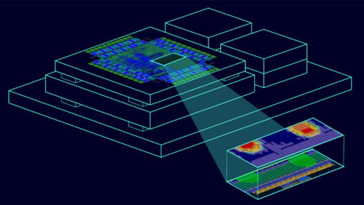
Realizing the strict design rule in the 32nm generation was originally seen as requiring dual exposure technology in the lithography process, which would result in higher process costs due to increased process steps, and in degraded manufacturing yields owing to increased process dusts. Toshiba realized an architecture based on single exposure lithography by applying ArF immersion lithography with a NA 1.3 and over, and by optimizing the lithography illumination conditions.
The development work also demonstrated that application of a metal gate/high-K not only boosts transistor performance but also reduces threshold voltage mismatch, which affects stable operation of SRAM and logic circuits. In addition, a bent-shaped type cell was selected for layout optimization, which also contributed to reduce threshold voltage mismatch.
By adopting this approach, Toshiba realized a 32nm CMOS platform design that reduces cost per function by 50% from 45nm technology, an achievement that would have been impossible with conventional poly/SiON and double patterning.
Toshiba will further enhance development of the new platform.
The achievement was introduced at the International Electron Devices meeting (IEDM) in San Francisco, CA.