









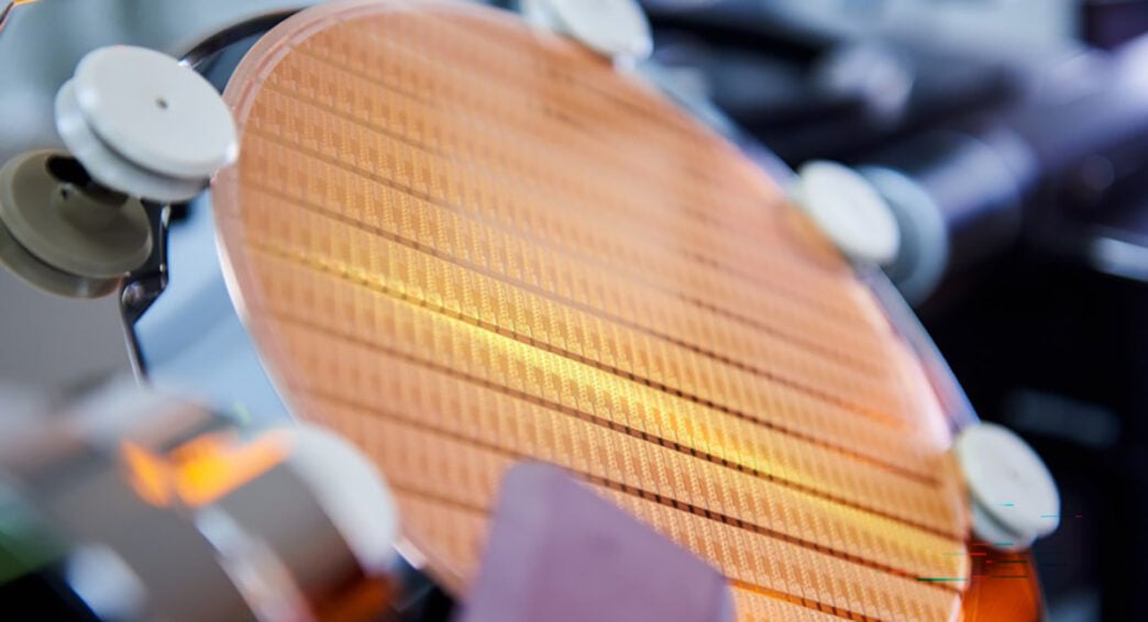
The global semiconductor supply chain is facing a critical friction point, but it is not due to a lack of demand for mature technologies. Instead, the challenge lies in a structural shift among conventional pure-play foundries. Many traditional manufacturers have stopped investing in their 200mm facilities, actively scaling down legacy capacities or repurposing their lines for advanced packaging and high-end digital logic. For automotive, industrial, and medical equipment manufacturers who rely on long-lifecycle applications, this divestment creates a severe and sudden risk of component obsolescence.
In stark contrast to this industry flight, X-FAB has adopted a dedicated specialty foundry strategy. Rather than abandoning mature nodes, X-FAB has continuously invested in and modernised its 200mm manufacturing facilities. This capital commitment does not just expand production volumes; it actively secures the long-term availability of specialised analog/mixed-signal processes for the next 15 to 20 years.
Consequently, the strategic priority for engineering teams is no longer about escaping 200mm but rather migrating their proven intellectual property (IP) away from unstable suppliers and into a secure, modernised 200mm ecosystem. Historically, this migration required a gruelling, manual translation of layout geometries that stalled time-to-market. Resolving this bottleneck requires a seamless interface where X-FAB’s robust PDKs and Cadence Virtuoso Studio’s software automation converge to seamlessly transfer legacy CMOS assets into long-term, production-ready silicon.
The IP preservation challenge
Why manual reverification and adjustment of legacy CMOS IP across process nodes traditionally stalls time-to-market
Unlike digital circuits that scale predictably through automated synthesis tools, analog, high-voltage, and sensor-rich mixed-signal designs are deeply tied to the physical characteristics of their original process node. When moving legacy CMOS IP from one manufacturing facility to another – even when the process node geometry remains identical – linear scaling and direct porting simply do not apply. Every foundry implements unique layout rules, toolsets, and device parameters that fundamentally alter circuit behaviour, modifying threshold voltages, transconductance, and matching properties.
Traditionally, this cross-foundry migration forces engineering teams into a punishing, manual redesign cycle. Layout designers must rebuild circuits component by component to comply with complex Design Rule Checking (DRC) and Layout Versus Schematic (LVS) requirements of the new node. Furthermore, smaller geometries introduce severe sub-micron parasitic effects, short-channel phenomena, and tighter voltage constraints that were non-existent in older processes.
As Joerg Doblaski, Director of Business Development & Technology Strategy at X-FAB, points out: “Many of our customers create their own libraries of building blocks on top of our rich design IP portfolio. The effort for re-creating the same set of design libraries can be a bottleneck when moving to a new process, so investing into an automated solution makes a lot of sense.”
Without automation, every adjustment requires iterative, months-long loops of manual layout modification, parasitic extraction, and circuit simulation. This unpredictable process routinely stalls time-to-market, increases engineering costs, and introduces high tape-out risks for critical automotive, industrial, and medical applications.

The automation framework
How the integration of X-FAB’s process expertise and PDKs with Cadence’s Virtuoso Studio delivers a ‘first-time-right’ automated design workflow
To overcome the friction points of manual migration, X-FAB and Cadence have integrated their technologies to create a fully automated, foundry-aware design workflow. This framework bridges the gap between old and new nodes by combining X-FAB’s comprehensive Process Design Kits (PDKs) with the advanced migration capabilities of Cadence Virtuoso Studio.
The automated workflow begins at the schematic level. Instead of manually resizing transistors and adjusting passive components, Virtuoso Studio automatically maps the legacy schematic parameters onto the target X-FAB process geometry. The tool optimises device dimensions to maintain original circuit performance, transconductance, and matching characteristics under the new node’s physical constraints.
Once the new schematic is validated, the automation extends to the physical layout. Using X-FAB’s precise routing rules and device models, the system automatically translates the original silicon layout into the target geometry. The software handles complex sub-micron design rules in real-time, automatically correcting potential DRC and LVS violations during the generation phase.
While acknowledging that a 100% automated layout migration for customised analog circuits down to 110nm is not yet fully possible due to routing diversities, Doblaski emphasises the immediate ROI: “Nevertheless, we consider the migration flow based on the Cadence tool set already a big step forward compared to a fully manual flow. Especially the sparse designer resources are freed up for working on new topics rather than supporting a manual design migration.”
By substituting traditional manual iterations with precise algorithmic scaling and continuous verification, this joint framework drastically cuts engineering timelines and ensures a ‘first-time-right’ tape-out.
Supply chain resilience
How efficient design migration acts as a strategic hedge against geopolitical risks and obsolescence in automotive, industrial, and medical applications
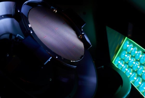
The global semiconductor landscape is experiencing a profound structural shift driven by geopolitical tensions and supply chain regionalisation. As mainstream foundry 200mm fabrication facilities face inevitable phase-outs and capacity constraints, the electronics industry must confront the reality of component obsolescence. For mission-critical sectors such as automotive, industrial, and medical equipment, an unexpected end-of-life notice for a single legacy integrated circuit can halt entire manufacturing lines and disrupt essential services.
This macroeconomic reality is driving concrete action. According to Doblaski, fabless companies worldwide are actively defining regionalisation strategies to reduce risks.
He notes that Asian foundry scale-downs of 200mm capacities heavily impact mature technologies still in high demand: “By supporting automated migration flows, we want to enable a smooth migration into our technologies, without heavy design work and with the goal to achieve ‘first-time-right design’ which can ramp quickly to volume.”
In this volatile environment, efficient process node migration serves as a powerful strategic hedge. Traditionally, moving a proven design to a different foundry or a more advanced geometry required a massive commitment of time and capital, often rendering proactive risk mitigation economically unviable. By removing these financial and technical barriers, the automated workflow enables companies to rapidly port their critical intellectual property to modern, secure process nodes before supply vulnerabilities turn into operational crises.
Ultimately, this agility transforms how manufacturers approach supply chain resilience and business continuity. The capability to seamlessly transition legacy analog and mixed-signal designs allows engineering teams to easily implement dual-sourcing strategies across different geographic regions. By cutting migration timelines from months to days, X-FAB and Cadence empower high-reliability industries to safeguard their product portfolios, protect long-term investments, and insulate themselves from macroeconomic shocks.
Conclusion
Embracing automation to secure the future of analog IP
The collaboration between X-FAB and Cadence marks a turning point in how the semiconductor industry handles legacy silicon. For years, the physical complexities of analog and mixed-signal design forced companies to choose between the high risks of supply chain obsolescence and the prohibitive costs of manual redesigns. By replacing slow, error-prone manual layouts with an automated, foundry-aware framework, this partnership eliminates that compromise entirely.
As the industry continues to navigate geopolitical shifts and the decline of mainstream foundry 200mm capacities, agility is no longer just an advantage – it is a survival requirement. Shifting the node migration timeline from months to mere days allows manufacturers to protect their intellectual property, implement robust dual-sourcing strategies, and ensure long-term production resilience. Ultimately, embracing this automated approach guarantees that the critical analog building blocks powering tomorrow’s automotive, industrial, and medical innovations remain secure, viable, and ready to scale.