


There’s an assumption in industrial EVs that smaller is always better. For 30 to 40 years, contactor miniaturisation has delivered steady progress. But high-voltage contactors have now hit dimensional thresholds dictated by voltage, thermal management, and arc suppression physics. These aren’t engineering challenges waiting to be overcome through better design. They’re physical constraints that define what’s possible.
Until something dramatic happens in materials science or fundamental switching technology, this is as small as contactors can realistically get. The conversation needs to shift from chasing millimetres to optimising what matters: robustness, reliability, and total cost of ownership.
Where the physics wall stands today
The dimensional limits of modern contactors are dictated by three immovable constraints, each rooted in electrical physics rather than manufacturing capability.
First is insulation distance, specifically what engineers call creepage and clearance. You need minimum air gaps and surface distances between live parts and ground to prevent flashover. These distances are driven by system voltage, pollution levels, and altitude. Below certain thresholds, the probability of partial discharge and tracking rises exponentially. Better materials can help at the margins, but they don’t erase the minimum distances required for a given voltage, environment, and standard.
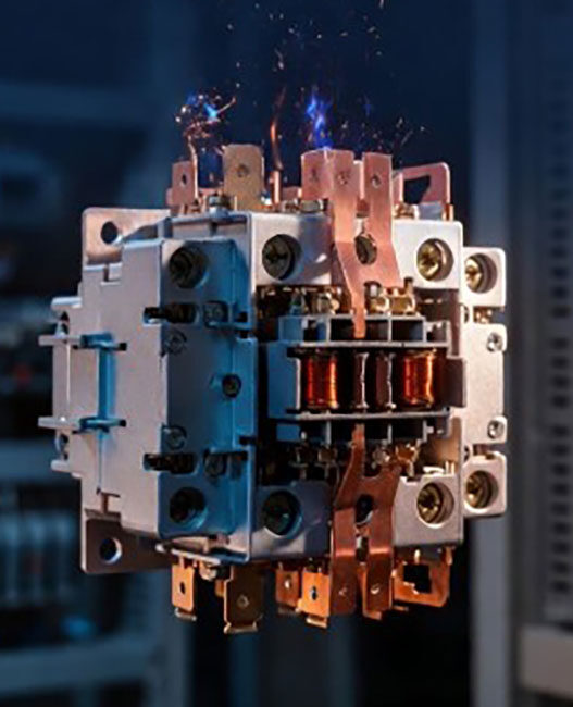
Second is arc length and contact gap. When contacts open under load, an arc is inevitable. That arc needs enough physical space to stretch, cool, and extinguish reliably. This requires adequate contact gap, controlled arc length, and active arc management through magnetic blowouts or inert gas chambers. Compress that gap too far and the arc doesn’t extinguish cleanly, especially under fault conditions. The result is accelerated degradation and reduced operational life.
Third is thermal management and conductor cross-section. High currents demand substantial copper mass. There’s no way around this. Without sufficient cross-sectional area in contacts and bus bars, temperature rise becomes excessive and internal components risk breakdown. The contacts must carry continuous current and handle short-circuit events without overheating or welding shut. This defines a minimum copper and contact material mass, plus enough thermal mass or cooling path to manage heat dissipation effectively.
When you combine these three constraints, you arrive at a box size that can’t shrink much further without increasing failure risk. You can optimise shapes and improve packaging efficiency, but for a given voltage and current rating, the basic distances, gaps and cross-sections don’t move much because of these physical limitations.
What happens when you push past the limits
The failures that emerge when manufacturers push contactors too small aren’t dramatic explosions on day one. Instead, you see subtle but serious reliability erosion in the field.
Insulation gets stressed closer to its limits, leading to increased partial discharge, tracking events, and occasional flashovers, particularly in humid or dusty environments or where condensation forms. Contact wear accelerates because shorter gaps and constrained arc paths create hotter arcs. Contacts pit and roughen faster, increasing resistance and temperature, which further accelerates degradation. This feedback loop drastically shortens operational life.
There’s also heightened risk of contact welding and stuck contactors when thermal limits are exceeded. Higher temperatures combined with high inrush currents can cause contacts to fuse together, creating dangerous failure modes.
Perhaps most concerning is the narrowing of the safe operating area. A contactor might pass laboratory tests on a clean bench under controlled conditions, but real-world deployment introduces tolerances, contamination, ageing effects and vibration. All these factors push marginalised designs over the edge.
Design choices that improve robustness
Accepting that contactors can’t get significantly smaller doesn’t mean design has stagnated. Within existing form factors, there’s substantial scope for optimisation, though every improvement involves trade-offs.
Contact materials and geometry can be upgraded. Advanced silver alloys and thicker contact layers increase arc resistance and reduce wear. Optimised contact shapes improve self-cleaning by wiping away oxidation layers that form during operation, reducing local hotspots. The trade-off is higher material cost, particularly given current silver and copper prices, plus increased manufacturing complexity.
Increasing conductor cross-sections and refining bus bar design, along with improving clamp forces, tightens resistance variation and improves thermal performance. But more copper means higher cost, increased weight and slightly larger terminals.
Upgrading to more robust plastics, advanced ceramics and improved seals enhances resistance to condensation and contamination. Again, material costs rise and, in some cases, outer dimensions or weight increase marginally.
Coil optimisation and electronic drives ensure reliable closing under voltage dips, fluctuations and high temperatures. Improved latching and return spring designs reduce contact bounce. These refinements add sophisticated electronics to the bill of materials and introduce additional heat from coil drives that must be managed.
Arc control systems can be enhanced through better magnetic blowout designs, arc chutes or inert gas selection. However, arc chutes add considerably to the size of the contactor itself, and in most cases the performance gain doesn’t justify the dimensional penalty.
When cost escalation stops making sense
The economics of pushing against physical limits don’t scale linearly. Costs rise exponentially as you approach boundary conditions.
Advanced contact materials, high-grade insulators and precision springs don’t add cents to the part cost. They add dollars. Supply is limited because demand is low, driving prices up. Scrap rates and yield failures worsen dramatically when targeting tighter tolerances. Producing springs with narrower resistance bands or contacts with lower variance requires manufacturing large batches, grading components and rejecting the majority that falls outside specification. The tighter the tolerance band, the higher the reject rate, inflating unit costs.
Testing and validation requirements also escalate. Making incremental design changes to improve performance demands more extensive testing across more units, more operational extremes and longer duration cycles. The engineering and laboratory costs per design iteration multiply rapidly, reaching a point where concepts become economically unviable regardless of potential performance benefits.
Technologies that could genuinely move the wall
The physics wall isn’t permanent, but shifting it requires genuine technological breakthroughs, not incremental improvements.
Advanced insulation materials such as next-generation ceramics, polymers, and composites offer higher dielectric strengths and improved tracking resistance, potentially helping to reduce creepage and clearance requirements. But adoption is limited. Early-stage suppliers are developing these materials, but market penetration is slow. It takes years for new material platforms to gain broad acceptance, achieve standardisation and reach cost parity with established alternatives. The battery industry offers a useful parallel: initial costs were prohibitive, but as adoption accelerated, manufacturing scale drove prices down. Contactors will follow a similar trajectory, but we’re in the early adoption phase.
Next-generation contact materials, including nano-structured surfaces and erosion-resistant coatings, promise reduced wear, enabling shorter gaps or lower contact mass without sacrificing operational life. Vacuum contactors offer superior arc quenching but remain niche products. Mass production techniques for vacuum contactors don’t exist yet, limiting their application to specialised high-value installations.
Hybrid architectures combining power semiconductors like silicon carbide or gallium nitride with mechanical contacts show promise. In these designs, semiconductors handle the high-stress switching transients while mechanical contacts carry steady-state current, dramatically reducing arc energy exposure. This allows smaller mechanical structures and improved thermal management, though at the cost of increased system complexity.
Additive manufacturing could also reshape packaging efficiency. 3D printing enables complex geometries that eliminate dead volume – the internal space that exists purely because conventional manufacturing processes require certain shapes. This technology accelerates prototyping and concept validation today, but materials suitable for reliable field deployment at scale require further development and extensive validation.
Stronger rare-earth magnets are improving arc quenching performance within existing footprints, though they introduce supply chain complexities and export control considerations.
The path forward
Until materials science or fundamental switching technology delivers a step change in capability, the dimensional boundaries of contactors will remain largely static from a cost-effective, mass-market perspective. That’s not an admission of defeat. It’s an acknowledgment of physical reality.
For battery-powered industrial EVs where every cubic centimetre counts, compact design remains critical. But for commercial vehicles, mining trucks and heavy-duty applications, the engineering focus should be on making contactors more robust within existing form factors rather than pursuing incremental size reductions that compromise reliability. For applications where packaging is genuinely constrained, existing compact contactors already push close to physical limits. The use of magnets serves as a clear illustration of how the industry has found ways to meet customers’ current needs. For everything else, specifying proven, robust designs with margin for real-world operating conditions delivers better outcomes than gambling on marginalised components that look good on paper but fail under stress.
Understanding where the physics wall stands and why it exists allows engineers to make informed trade-offs rather than pursuing unattainable miniaturisation goals. The future of contactor technology lies in material science breakthroughs, hybrid architectures and advanced manufacturing, not in shaving another millimetre off existing designs. Recognising this distinction is how the industry moves forward intelligently.
This article originally appeared in the February’26 magazine issue of Electronic Specifier Design – see ES’s Magazine Archives for more featured publications.