


Eric Aguilar, Co-Founder and CEO, Omnitron Sensors, has a bachelor’s degree in electrical engineering and in his early career he was a team member at US Navy Research Labs who developed a low-cost accelerometer-gyro. Eric switched from sensor developer to sensor integrator in the next phase of his career.
Leading teams at companies such as Project Wing at X (Google) and Tesla, Eric saw first-hand that the operational cost of sensors for LiDARs. “In some cases, the optical subsystems for scanning mirrors were frail and expensive. At times, these failures required the replacement of the LiDARs in cars every three to six months.
“Calibration was also a serious issue, creating another point of potential failure in LiDARs. No one wants to take a car to the shop frequently because of a faulty LiDAR system. I saw this as a huge obstacle to the growth of autonomous vehicle technology.
Given my experience in MEMS and in sensor integration – and the phenomenal technical experience of our other founders – I believed we had what it would take to revolutionise MEMS scanning for LiDARs.”
Here, Electronic Specifier’s Sheryl Miles talks to Eric about their new topology for MEMS and what this means for the future of LiDAR.
What does Omnitron do?
At Omnitron we’ve developed a “new topology for MEMS.” It starts with test structures and process steps, developed at foundry partners. We’ve made significant improvements in capacitance to produce robust, rugged devices. And we’ve verified our process through fabrication. We don’t require new semiconductor or MEMS tools in the fab. We’ve rearranged processes, and we are on the path to build hundreds of millions of low-cost, reliable, repeatable MEMS devices at commercial MEMS foundries.
The first proof point of our new topology for MEMS is our optical subsystem for LiDARs. It’s a MEMS step-scanning mirror.
Can you explain how the MEMS step-scanning mirror works?
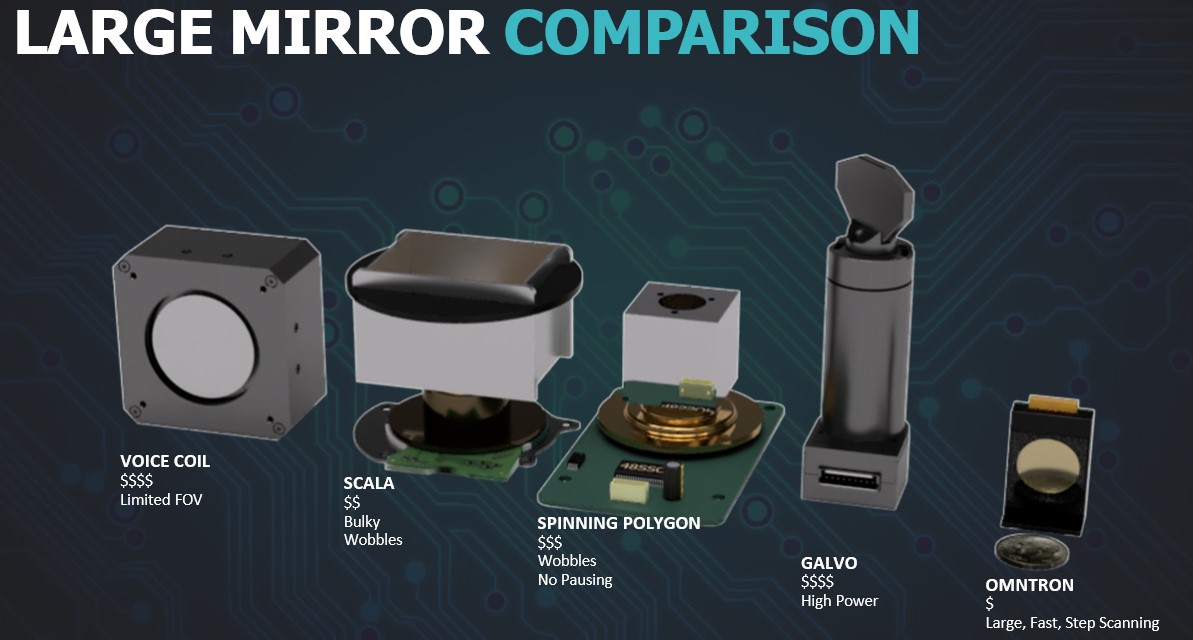
I’ve learned from the LiDAR industry that companies need a big mirror, something with about 10mm diameter. Existing MEMS mirrors are about 1-2mm, so they can’t meet LiDARs’ requirements.
The newest spec for LiDARs is FMCW (frequency-modulated continuous wave) resolution. That means you need to stop the mirror in a step fashion so it’s not just resonating (or spinning), which is how older technologies are structured.
A MEMS step-scanning mirror, on the other hand, allows us to measure the position of the mirror in real-time. We’ve improved capacitance per unit area by building a much bigger MEMS motor. More specifically, our topology can build a large 15mm in diameter mirror with tens of degrees of motion and the ability to do step scanning. Customers are excited about our approach.
What are the improvements over other optical subsystems?
Customers need a big, fast, robust mirror that does step scanning. Spinning polygons are the most common solution now, but they’re expensive and prone to wobble – which throws off the calibration. Voice coils, used in satellite systems, are $5K each – so way too expensive for LiDARs used in automotive, robotics and drones. The Galvo has a huge mirror behind it to do the step scanning, but it’s also very expensive and high-power. In an automotive environment, OEMs need a small, sleek LiDAR that fits in the roofline. Our MEMS step-scanning mirror doesn’t have the issue with wobble because it’s a step-scanning not a spinning device – and it’s tiny, about the size of a dime.
How does the MEMS scanning mirror alleviate LiDAR’s optical-detection issues – as well as reduce size, cost, robustness, and reliability problems?
- We’ve built a huge motor (very powerful actuator) – one that’s 10x better than competitive scanning approaches.
- We’ve built a step-scanning mirror that’s not prone to the same technical problems as spinning mirrors. This dramatically improves accuracy and reliability. We do this in two ways, providing isolation from the drive electronics to sensing electronics and enabling direct measurements of the physical position of the mirror. This dramatically improves accuracy and reliability, which translates to higher probability for detection of a target, thereby improving LiDAR optical detection.
- We’re using existing tools and capabilities, which again, reduces cost and speeds time to market. We came up with a clever sequence to achieve much higher performance. The result is great uniformity across the wafer with a robust process for fabrication that’s also simple. This keeps costs low.
How have you streamlined process technology and packaging techniques to speed mass production of MEMS for high volume markets?
We can do the offsets at the wafer-level, so everything’s planar. This is huge for the system-level calibration and assembly process. The BOM is not expensive. It’s the active alignment step that’s the most expensive step in LiDAR. We simplify that active alignment step.
We use existing tools, so our process doesn’t require new, expensive tools at the foundry. Rather, part of our IP is that we use existing tools while cleverly rearranging the process steps in MEMS manufacturing.
What applications are best suited for the MEMS mirror?
LiDARs for autonomous systems in automotive, drones and robots.
What challenges have you encountered?
Scaling! We’re fortunate to benefit from the inherent ability to batch-level fabricate our tech, which allows for high-volume production. We’ve been able to prove our process at R&D fabs, leveraging volume production processes and tools. Now we’re moving toward running at foundries that have the volume capacity that our market demands. We’re actively looking for the right foundry partnerships now.
What have been your highlights?
The reception that we’ve received from Tier I LiDAR suppliers has been our chief highlight. Our customers want to buy our MEMS step-scanning mirror. This is closely followed by receiving third-party verification of our MEMS process. Our process works as intended, and earning independent verification is a milestone that we’re proud to have achieved.
What’s next?
Releasing our MEMS step-scanning mirror in samples to our customers and proving out manufacturability.