
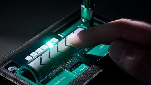


Paragraf and Archer Materials are coordinating on a project to develop a world-first graphene-based quantum computing device.
A world first
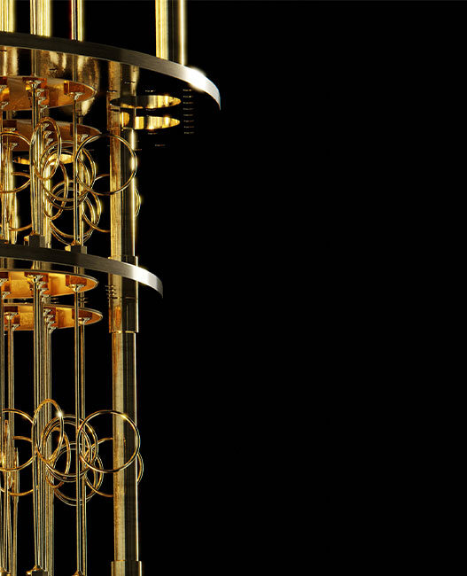
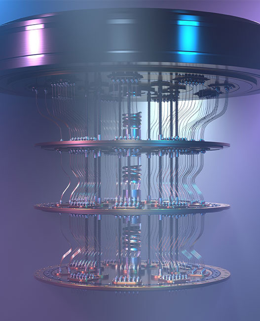
Quantum computing is a fast-growing and ambitious industry. Yet, for all the progress made with silicon-based systems, ion traps, and superconducting circuits, the materials challenge is one of the biggest hindrances to scaling the technology. The cooperative and development programme announced by Paragraf and Archer Materials is seeking to move this stoppage to scalability and transport next-generation quantum computing hardware into the big leagues with graphene-based device platforms.
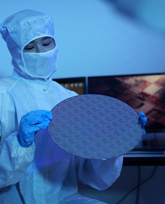
While other carbon nanostructures, such as quantum dots, carbon nanotubes, nanodiamonds, and flakes of exfoliated graphene, have been explored in quantum, these structures are small and hard to locate and work with, Rosie Baines Warburton, Key Account Technical Lead at Paragraf tells me. Not only this, but none of them have been incorporated into a device architecture in the way this programme intends. “Demonstrating a manufacturable and scalable graphene-based device that can interface with quantum computing systems would be a first,” says Baines Warburton, “and would show that the promise of graphene for quantum applications is one step closer to being realised.” The platform Paragraf is using is wafer-scale graphene, deposited directly onto the device base, and designed to be manufacturable within standard semiconductor processes.
What Archer Materials brings to the table
Archer Materials brings domain expertise in device physics, quantum materials, and sensing application development, which is a complement to Paragraf’s strengths in scalable graphene growth. “Archer have been working in the quantum space for some time, and they have a level of expertise that is useful for developing solutions for quantum computing applications,” says Baines Warburton. “They are experts in characterisation, testing, and analysing quantum tools, all of which will help with learning more about graphene’s capabilities.”
With their combination of skills Paragraf can contribute a commercially scalable graphene platform, and Archer can contribute to knowledge of the device physics that is needed to turn that material into something that functions within a quantum system. “This collaboration reflects our strategy of partnering with world-class technology developers to unlock the potential of advanced materials,” said Simon Ruffell, CEO of Archer Materials. “Graphene offers unique advantages for both quantum devices and sensors, and Paragraf’s platform provides an exceptional foundation to realise those advantages in real-world devices.”
Tackling scalability
Scalability is a big challenge when it comes to quantum computing. “There are various technology platforms for quantum technology being explored. Silicon-based platforms and ion traps are two of the more established, but they face scaling challenges, and it is likely that advanced materials will be needed to truly unlock quantum computing, realising its full potential,” says Baines Warburton.
Graphene has exceptional electronic mobility, low noise characteristics, and atomic-scale thickness, but most importantly for this project, its potential to maintain robust quantum states means that it is a material capable of supporting more error-tolerant quantum systems, which in turn could allow for scaling to higher qubit densities. “Of those materials, graphene shows particular promise because of its potential to maintain robust quantum states,” says Baines Warburton. “The ability to produce high-quality graphene at scale will allow this potential to be exploited in the application space.”
The programme is based around research into novel graphene device architectures for qubit detection, including graphene structures capable of interfacing with emerging quantum systems. “Our graphene technology was developed to be manufacturable at scale while maintaining the exceptional properties of graphene,” said Simon Thomas, CEO of Paragraf. “By working closely with Archer Materials, we are able to explore advanced device concepts in both quantum detection and computing that extend the capabilities of our platform.”
A commercially viable product
The Paragraf–Archer collaboration is anticipating multiple iterations of designing and testing new device versions on the path to any commercial outcome. “The success will come in learning how to build a graphene quantum computing device. The data we generate through this project will tell us a lot about our graphene’s capabilities and about the tools required to manage qubits effectively,” says Baines Warburton. “A real, marketable graphene quantum device that can be put to work in commercial-grade quantum computers will, of course, be a mark of great success for this process. There are many milestones to achieve and many lessons to learn along the way.”
The typical end customers for quantum computing tools are currently concentrated in the research community, like large universities, government-backed research bodies, and the R&D departments of major corporations. But the longer-term market could be far larger. “Existing quantum computers require significant resources (e.g., space, power, cryogenics, etc.), so it may seem like they will never leave the confines of those large research institutions. However, the same view was taken of large mainframe classical computing systems before – and even, for a while, after – the advent of the desktop PC. The possibilities for next-generation quantum computing that could overcome these challenges are limitless,” says Baines Warburton.
When asked why graphene should be taken seriously as a viable option for scaling quantum hardware compared to other approaches, Baines Warburton says that the landscape has shifted: “Quantum computing is still an emerging technology, being demonstrated as advantageous over conventional computing currently in limited scenarios, and with multiple platforms being explored. There is currently no general-purpose quantum computer and no front-running technological route. The properties of graphene, particularly the ability to maintain robust quantum states, make it a clear contender for exploration, and the ability to manufacture it at scale makes it a viable option rather than limited to the research lab.”
Much theorising about graphene in quantum applications has taken place before, and some graphene-adjacent materials have even been put to use. But this is the first time directly deposited, wafer-scale graphene will be incorporated into this class of device architecture. The empirical data generated over the coming months will, for the first time, show concretely how this material performs under these conditions.
The reality for graphene
Asked whether this partnership means that graphene is finally making the transition from promise to practice, Baines Warburton says. “By launching multiple graphene-enabled products and opening the world’s first graphene foundry, we’ve already demonstrated that graphene has moved from potential to reality. We have created devices that harness graphene’s unique electrical properties, proven our ability to manufacture them at scale, and have customers across many different industries. This collaboration represents an opportunity to explore the benefits of graphene for quantum computing via proof-of-concept devices that can be manufactured using standard semiconductor processes.”
For Paragraf, this collaboration could lead to the demonstration of transformative devices and, in time, to a deeper understanding of how graphene can be employed across a quantum system. “This project is hopefully the first step in a collaboration that will lead to the demonstration of revolutionary devices and allow both parties to gain a deeper understanding of how graphene can be employed in a quantum system,” says Baines Warburton. Both Paragraf and Archer Materials expect the programme to generate a pipeline of differentiated graphene-based technologies addressing emerging markets in quantum computing, advanced sensing, and next-generation electronics.