


Realise the potential of automotive SiC MOSFETs
INTRO
Some of the limitations of SiC MOSFETs can be countered with the use of suitable packages, propose Christian Felgemacher, Felipe Filsecker, Farhan Beg and Aly Mashaly, Rohm Semiconductor and Seiya Kitagawa, Rohm
While silicon carbide (SiC) MOSFETs can achieve very high switching speeds which helps to reduce the energy loss in power electronic converters significantly, the full potential of the devices cannot always be used due to limitations of the traditional power semiconductor packages.
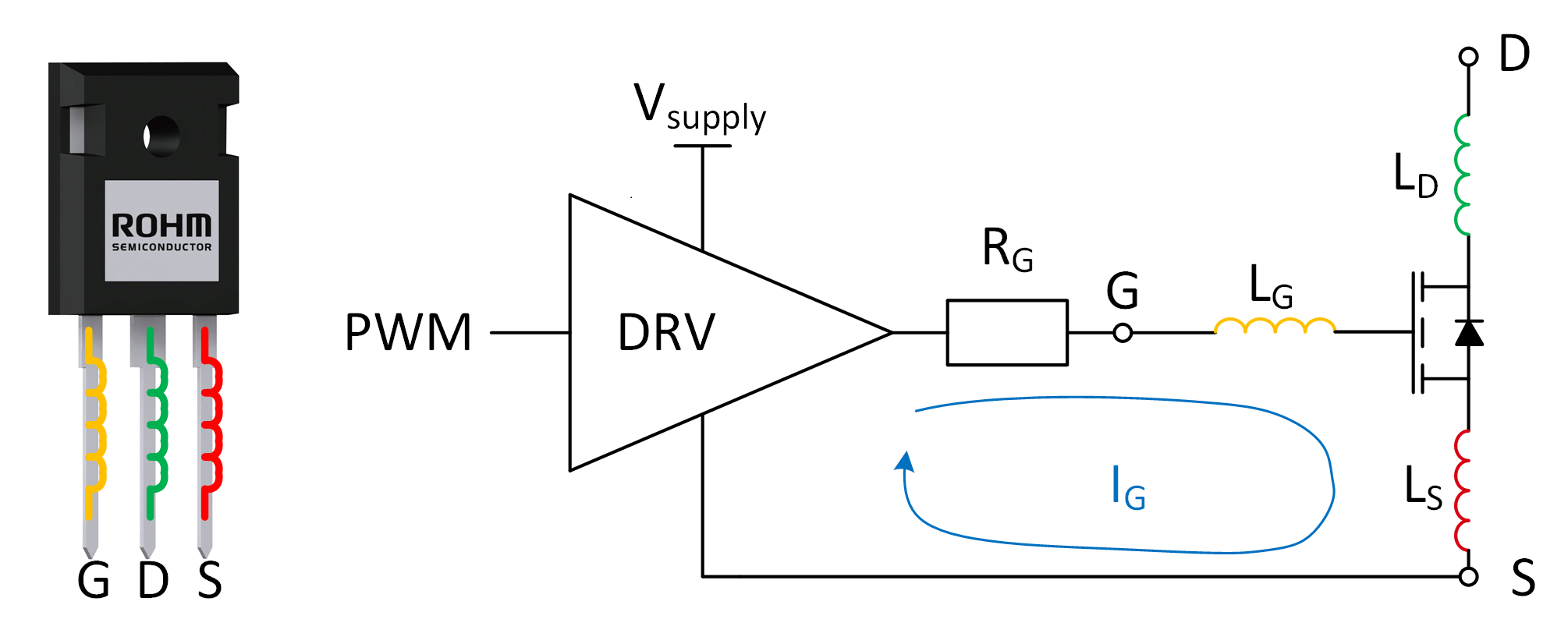
Figure 1: Traditional power device package and its parasitic inductances
Figure 1 shows one of the most widely used traditional packages for power transistors, the TO-247. Each leg of the device presents a parasitic inductance element. These have been added to a very simple representation of a typical gate drive circuit, showing that the inductances of the drain and source pins add to the loop inductance in which the main current is switched. This causes over-voltage at turn-off. As a result the switching speed needs to be limited to ensure that the specifications are not exceeded.
The parasitic inductances of the gate leg and of the source-leg are part of the gate-drive loop. This impedance has to be overcome when driving the MOSFET. Additionally, oscillations between this inductance and any parasitic capacitances in the gate drive circuit can occur. Source inductance (LS) is present in both the power loop and the gate loop the inductive voltage drop (VLS) across this inductance during turn-on of the MOSFET (as a consequence of increasing IS) reduces the effective gate voltage, which slows down the turn-on of the MOSFET (see Figure 2).
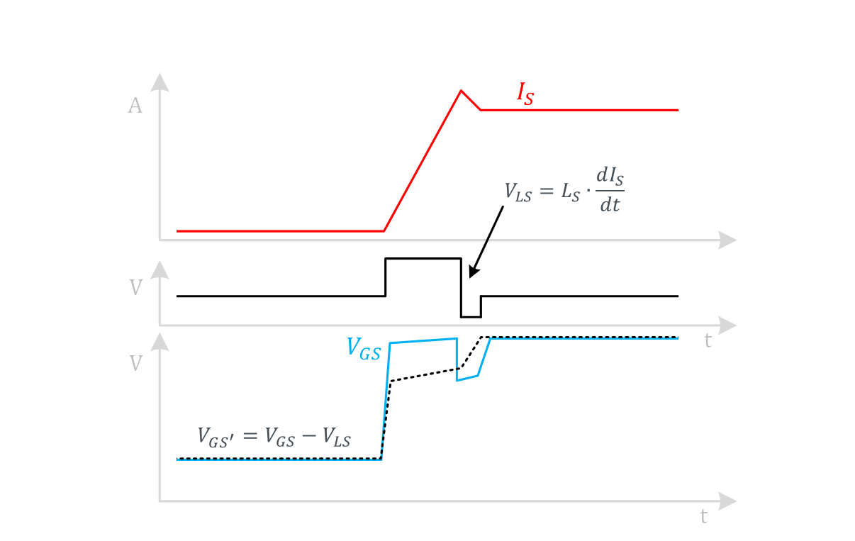 Figure 2: Gate source threshold voltage (VGS) at chip is reduced during turn-on due to LS
Introducing the Kelvin Source pin to the TO-247 package offers significant improvement by separating the gate drive loop from the power source terminal. As a result, the turn-on is not slowed down by a voltage drop due to the rising source current, leading to significant reductions in turn-on losses.
SMD packaging
Rohm Semiconductor is extending its portfolio of discrete SiC MOSFETs with automotive qualified devices in the TO-263-7L SMD package. The benefit of the Kelvin connection to the source terminal of the SiC MOSFET provided by the TO-263-7L package is illustrated in Figure 3. It can be seen that the main source-inductance LS is no longer shared by the gate-drive loop and the main current path. As a consequence, the device can be turned on faster which leads to reduced turn-on loss.
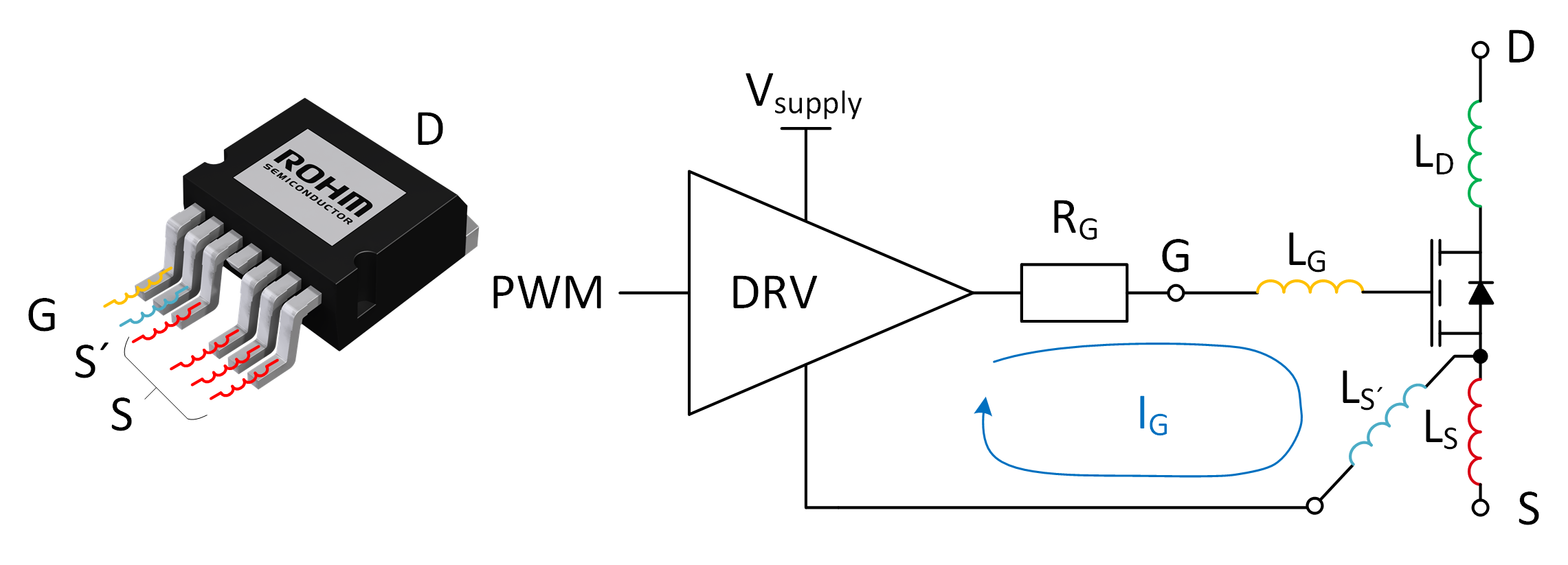
Figure 3: The TO-263-7L SMD package and its parasitic inductances
Another benefit of the package is that it has much lower stray inductances than the TO-247 package and its variants.
At turn-on, the three-lead device is limited in terms of switching speed because the inductive voltage drop across the source terminal reduces the effective gate voltage leading to a long period at the Miller plateau which causes significant turn-on losses. This period is shorter in a device in the SMD package with Kelvin Source connection to the gate driver and hence the turn-on loss is reduced. A much higher dI/dt can be achieved in the SMD package, due to the reduced parasitic inductance and hence the turn-off loss is also less than in the TO-247 package.
In the below diagram the switching energies achieved for both devices are shown as a function of switched current. It becomes apparent that at higher current the benefit of increased turn-on speed of the device in TO-263-7L is most relevant.
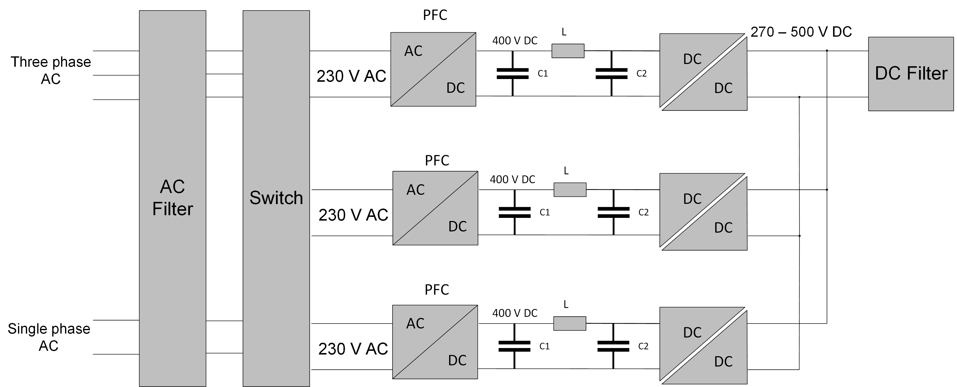 Figure 4: Block diagram of 11kW onboard charger, using multiple 3.7kW PFCs
To illustrate the performance that can be achieved with SiC MOSFETs in SMD packages, consider the application example of a 3.7kW single phase PFC stage. A single-phase PFC with such a power rating can be employed as the input stage for a single-phase 3.7kW onboard charger or as a building block for an 11 kW three phase on-board charging system. In the latter case three single-phase PFCs can be combined using a switching matrix at the input to allow for either single phase or three phase operation of up to 11kW. This approach is illustrated in the block diagram in 4.
PFC topologies
The classical boost PFC has limits in terms of the achievable efficiency due to the presence of the diode rectifier at the input. In the two phase bridgeless PFC as well as the two variants of the totem pole PFC, this input rectifier is eliminated which reduces the overall conduction losses. The two phase bridgeless PFC enables high efficiencies, but has the downside that each leg is only used during half of the input cycle. As a result, large power cycling stress is imposed on the power semiconductors and the ratio of peak current to RMS current of each devices is high.
Two different types of the totem pole PFC can be realised. In the simplest case, two transistors and two diodes are used. The diodes switch at low-frequency and hence devices with low forward voltage drop are selected. Since the body diodes in the transistors are used for commutation it is important to select devices with body-diodes that can be used in hard commutation. Modern wide bandgap semiconductors, such as SiC MOSFETs, have body diodes that are usable in hard switching making them a good choice for this application. Finally, if the highest possible performance is desired the losses can be further reduced by replacing the diodes in the low-frequency leg with active switches such as super junction (SJ) MOSFETs.
In a totem pole PFC simulation, the measured switching energies for a 650V SiC MOSFET with 60mΩ on resistance in a TO-263-7L were considered. A switching frequency of 100kHz was assumed and the semiconductor losses of the high frequency leg as well as the low frequency leg were modelled. For the latter, only the conduction losses of a 60mΩ device were considered, as negligible switching losses occur.
The results of this simulation was that maximum efficiency is in the region of 98.7% at around 60% of nominal output power, without additional losses being modelled at this stage. Developers should also consider losses in the inductor and other passive components as well as the control and gate-driving circuits, nevertheless, it is apparent that a high performance PFC can be realised with the totem pole PFC using 650V SiC MOSFETs.
Conclusion
The performance benefits which arise from the use of a low-inductive SMD package with a Kelvin-Source pin for fast SiC MOSFETs have been shown. Additionally, at high currents the turn-on loss in the SMD package is significantly reduced as the gate loop is not impacted by the dI/dt and the resulting voltage drop across the source terminal inductance. The overall reduction in package inductance allows much higher turn-off speeds for the SiC MOSFET. These advantages together result in significant reductions in the turn on and turn off energy losses. On the system side we have seen that 650V SiC MOSFETs with RDS(ON) values in the region of around 60mΩ in a totem pole PFC result in conversion efficiencies in excess of 98%. This enables very compact designs, which are particularly important for the development of onboard charging systems in automotive applications.
PCIM Euope Visit Rohm – Hall 9-312