


Si MOSFETs typically have an avalanche rating allowing them to operate beyond their maximum drain to source rating. In contrast, eGaN FETs do not have an avalanche rating but operate up to 120% of the maximum drain to source voltage for transient events. The main concern for GaN transistors operating beyond the maximum drain to source rating is dynamic on-resistance.
The traditional test is to apply maximum-rated DC Vds at maximum-rated temperature (typically 150°C). If no failures occur after a certain amount of time, the product is considered good. EPC has developed a first principle physics-based model to explain RDS(on) rise in GaN transistors under hard switching conditions.
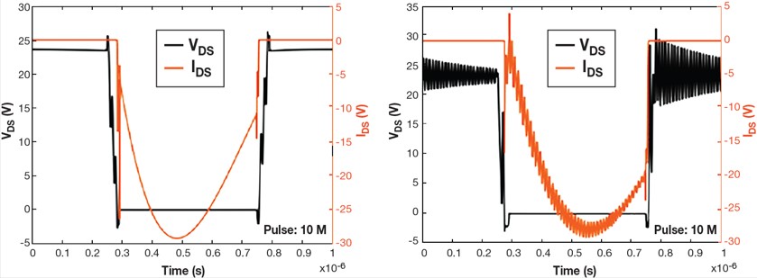
Figure 1. Low and high over-shoot cases for an LLC converter
It predicts RDS(on) growth with time and that the slope of RDS(on) over time has a negative temperature co-efficient (i.e. lower slope as temperature rises). It also predicts that switching frequency does not affect the slope but causes a small vertical offset and that switching current does not affect the slope. The following demonstrates two synchronous rectification application examples.
A realistic SPICE model was developed for the application circuits based on EPC’s reference designs, including the effects of parasitic layout inductances. These parasitic inductances are the main contributors to ringing and voltage over-shoot which can impact dynamic RDS(on) in the GaN device. The value of these parasitic inductances was increased to mimic the effects of poor PCB layout. The SPICE simulations captured channel current and drain to source voltage during one switching period, at steady state.
These single-cycle current-voltage loci were applied into the hot electron trapping model (implemented in MATLAB). This model calculates the charge trapping that occurs in each switching cycle, and determines when (e.g. turn on or turn off transitions) the most charging occurs. Integrating this model over the 10 year projected continuous operation of the application with identical switching cycles allows the cumulative charge trapping that occurs to be calculated. The instantaneous trapping rate depends (non-linearly) on the cumulative trapped charge, therefore the amount of charging per cycle is not constant but rapidly self-quenches over time as the FET switches.

Figure 2. Low and high over-shoot for a sync buck converter
Regions within a switching waveform that are most detrimental can also change as the device operates. This is automatically taken care of during integration of the model. The first example uses an output stage of 48 to 12V LLC converter (commonly used in server and AI applications). A SPICE model was developed to include the main layout parasitic inductances based on the EPC9149 demonstrator. By changing L1…L4 it was possible to change the over-shoot seen by the output stage devices. The calculations of voltage, current, and RDS(on) for the entire sequence of switching waveforms were made, with the amount of trapped charge QS calculated and summed with all previous cycles.
The calculation assumed the use of 40V devices and no increase in RDS(on) over the 10 year lifetime of the application for both low and high over-shoot cases. Repeating the exercise with 30V devices, there is no increase in RDS(on) during the 10 year lifetime for both low and high overshoot cases. Users can therefore consider using 30V eGaN FETs in this application without worry of dynamic RDS(on) increase due to voltage over-shoots. For the second example, a synchronous FET of a 48 to 12V buck converter was looked at operating in continuous conduction mode at 500kHz. A SPICE model was developed based on the EPC9078 demonstrator (see Figure 3 below).
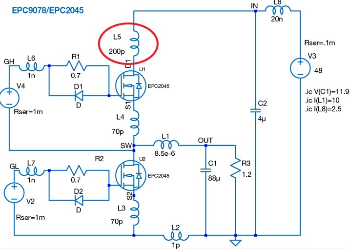
Figure 3. 48V – 12V synchronous buck converter operating at 500kHz
The conditions analysed for the low side synchronous eGaN FETs are with over-voltage of 50 and 90V (170V peak) – well beyond normal application conditions. The results, assuming the use of a 100V eGaN FET, is minimal RDS(on) increase with 50V over-shoot, while there is a more significant degradation when the device sees 170V peak voltage. These two examples illustrate that it is possible to clearly quantify the effects of dynamic RDS(on) depending on use conditions.