


This article originally appeared in the May’23 magazine issue of Electronic Specifier Design – see ES’s Magazine Archives for more featured publications.
GaN offers application benefits for several reasons. Firstly, it does not have a reverse recovery current, permitting simpler architectures to be used (e.g., totem pole for PFC). Secondly, it can operate at a higher frequency than silicon, enabling smaller passives to be used. The specific on resistance of GaN is much higher than silicon, so GaN device can be smaller. Lastly, GaN’s figure of merit (Ron x Qg) is 10 times better, resulting in much higher efficiencies.
Innoscience introduced bi-directional GaN (VGaN), the over-voltage protection unit in a battery management system requires two back-to-back silicon MOSFETs to block the current in both directions. These can be replaced by one VGaN HEMT for a solution that is 50% smaller and more efficient.
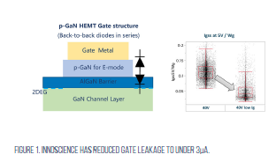
A silicon device normally has a blocking oxide below the gate to block the gate leakage. In GaN, this oxide layer is not present, so a two-diode back-to-back architecture is used (see Figure 1). By optimising the epitaxy, the processing and the architecture, Innoscience has reduced the leakage characteristic by nearly 10x, to under 3μA at 85°C for the device’s lifetime, making VGaN HEMTs suitable for use as the load switch inside mobile handsets.
Regarding price and the availability, it becomes clear why GaN has not yet been present in the mobile phone market. Assuming a 10% market penetration of the one billion phones sold in 2022, equates to 100 million GaN devices per year, requiring approximately 3,000 eight-inch wafers per month. Today, the total worldwide capacity of GaN, without Innoscience, is around 9000 wafers per month, according to Yole Group, therefore, mobile phones would require 33% of the worldwide capacity. Innoscience is an IDM (integrated device manufacturer) 100% focused on GaN. It can optimise design and manufacturing technology in-house without legacy silicon products to divide investment and capacity. It can provide eight-inch GaN wafers, cost-effectively in high volumes using two fabs. By 2025 the company will produce70,000 eight-inch wafers per month.
Reliability
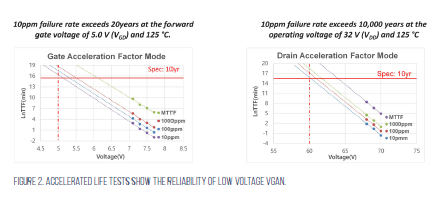
Innoscience’s devices are tested to JEDEC standards and accelerated life tests show that 10ppm device failure rates for gate acceleration factor mode exceed 20 years (Figure 2); for drain acceleration factor mode the figure is greater than 10,000 years.
Avalanche ruggedness of silicon power MOS devices is an important characteristic, which is typically measured by unclamped inductive switching test. The tested device is first turned on charging the inductor at a linear rate. When the required drain current is reached, the tested device is turned off causing the inductor to dissipate all of its stored energy and driving the tested device into a breakdown voltage. The avalanching capability of the tested device allows to dissipate the inductor current and thus limiting further increase of the voltage across the device. The tested device will remain in breakdown until all the energy is dissipated.
The results can be translated into time-in-avalanche and energy-in-avalanche that the power device can support. If the device does not have an avalanche capability, the power device must have much higher breakdown voltage to allow complete discharge of the inductor’s energy. In the Innoscience’s low voltage GaN devices, the breakdown voltage is more than twice the device’s rating and thus able to safely handle voltage spikes.
Data centres
Data centres is a growing market that is power-hungry. Therefore, efficiency is top priority and every 0.1% of increased efficiency that can be achieved will result in significant cost savings. Size is important as smaller power conversion systems frees up more space for computing units. Again, large, available product capacity and low price are essential.
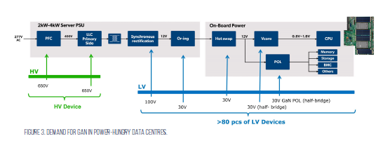
Figure 4 shows the power conversion stages inside a data centre, starting from AC/DC. A typical PFC and LLC design at the primary side will normally use 650V devices. But on the low voltage side, we see many 100V and 30V parts when we get down to the point-of-load devices. This will easily add up to around 80 low voltage power transistors per implementation, which must all be delivered in volume and at the right price.
Using four of Innoscience’s 3.2mΩ 100V GaN INN100W032A HEMTs in a 600W full-bridge LLC design results in a converter that is 25% the size of the equivalent silicon but is also 0.6% more efficient.
In addition to moving from discrete silicon MOSFETs to GaN HEMTs, further size reductions can be made by using an integrated solution. For example, a complete half-bridge circuit using the ISG 3201 integrates two half-bridge GaN HEMTS, the driver and the bootstrap capacitor in one LGA package measuring 5.0 x 6.5 x 1.1mm which is a size reduction of 20%.
The same 600W 48/12V DC/DC converter in the same data centre application, using the ISG 3201 will increase the power density and achieve 1000W in the same size module at an elevated efficiency of 98.26%.
To address the high voltage sector, 650V InnoGaN HEMTs ranging from 30mΩ RDS(on) to 80mΩ, 140mΩ and 190mΩ to 2.2Ω are available. GaN devices avoid avalanche failures by having a much larger breakdown voltage than the specified voltage rating. These 650V-rated devices report maximum drain-source voltage transient strikes for the device to withstand non-repetitive pulses below 200μs at 800V, well above the maximum rating.
For repeated pulses with a duration of less than 100ns, the maximum transient voltage the parts can sustain is 750V at room temperature and at 125°C, both well beyond the 650V rating. Multiple sources of GaN parts are emerging. For example, the INN100W032A is footprint- and pin-to-pin-compatible with the EPC 2218 with comparable performance and Innoscience’s 650/700V devices are pin-to-pin compatible with Infineon/GaN Systems parts.
Packaging
In addition to DFN (dual-flat no-leads) packaged devices, many applications use a single-sided PCB featuring power semiconductors in traditional packages. Innoscience has introduced devices in TO220/TO252 packaging that range from a RDS(on) of 140mΩ RDS(on) to 350mΩ (TO220) or from 190mΩ to 800mΩ (TO252). Tests show that at 100kHz, the efficiency of the GaN parts in DFN and TO2xx packaging is very similar. At higher frequencies, the difference will be more apparent, but for many applications TO2xx packaging can be used.