
Cameras cannot weigh down vehicles
Redesigning MOSFET packaging helped Rohm to meet the demands of automotive cameras for high current handling capability
Advanced driver assistance systems (ADAS) is being developed for practical realisation in many countries around the world. Onboard cameras play an important role in the configuration of these systems. Cameras mounted at the front, rear, left, and right of the vehicle allow drivers to view the surrounding environment on the instrument panel, significantly improving safety for driver, passengers and other road users.
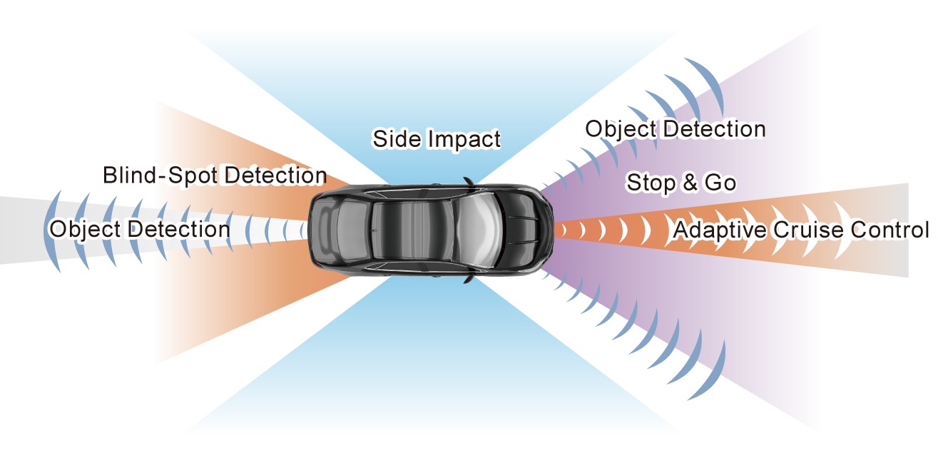 Figure 1: Onboard camera locations
The number of vehicle cameras is expected to increase three-fold by 2025. The reason for this rapid expansion can be attributed to not only the growing number of camera-equipped vehicles, but an increase in the number of cameras used per vehicle as well. A number of today’s vehicles incorporate four cameras, but this is sure to increase as functions such as ADAS become standard and more sophisticated (Figure 1).
Miniaturisation
Recent years have seen a demand for more compact vehicle cameras. This is largely due to the increasingly smaller available installation space, following the trend towards electrification, coupled with the growing number of cameras mounted per vehicle to further improve safety. Decreasing the size of automotive cameras allows for greater flexibility regarding the mounting position/location, minimally impacting vehicle designs.
Current cameras are mounted on a circuit board with outer dimensions measuring 20 x 20mm. In the coming years even smaller iterations are sure to be developed. At the same time the size of PCBs is shrinking, which in turn demands smaller components.
Increasing functionality and higher resolution, however, require larger currents. In addition, components to protect against reverse connection are being mounted to prevent damage to the camera system in the event a reverse voltage is applied to the power supply line. In the past, Schottky barrier diodes (SBDs) were used, but with high VF SBDs heat generation becomes problematic at large currents. As a result, many designers are replacing SBDs with MOSFETs that generate much less heat.
Package choices
Rohm supplies small-signal MOSFETs featuring a bottom terminal package. This increases the electrode surface area during solder bonding, minimising heat generation even if high power is supplied. The result is significantly higher power handling capability over conventional leaded packages, claims the company.
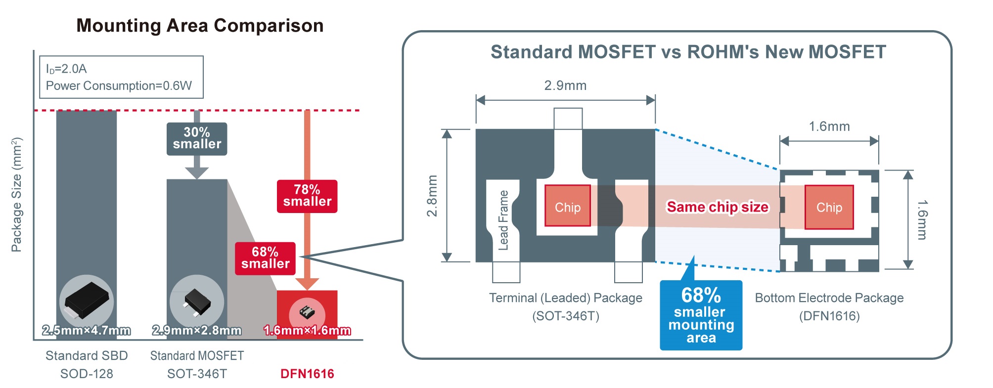 Figure 2: Comparison of the compact MOSFETs for reverse connection protection
The company’s latest MOSFETS, the RV4xxx series are optimised for reverse connection protection and offered in the compact bottom electrode DFN1616 package. With dimensions of 1.6 x 1.6mm, the MOSFETs meet the demands of automotive cameras for high current handling capability in a compact size. The result is 78% smaller mounting area over conventional SBDs and 68%, even when compared to standard leaded MOSFETs with the same specifications, reports the company.
During development, engineers discovered that, with the conventional DFN1616 package, it is difficult to verify solder condition via visual inspection after mounting. To solve this problem, designers have used wettable flank technology. This is a technique for plating the sides of the lead frame. Products using this technology exhibit superior toe fillet formation after mounting. The greater the height of the toe fillet the easier it is to verify solder conditions during visual inspection, improving mounting reliability (Figure 3).
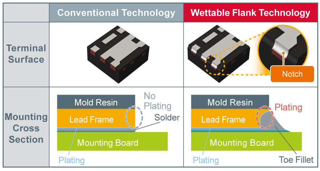 Figure 3: Wettable flank construction
In the automotive market in particular demands high mounting reliability, therefore a minimum solder height is required. Normally, forming a wettable flank involves cutting a notch into the lead frame using a blade before carrying out the plating process. The depth of this notch can significantly affect the height of the toe fillet after mounting. To achieve a consistent toe fillet height this notch must be sufficiently deep, but unfortunately the amount of burrs increases in proportion with this depth.
To add to the design challenge, when mounting, these burrs become part of the mounting surface, possibly causing package tilt or even connection failure. For larger packages this poses no problems, but the smaller the package, the greater the susceptibility (Figure 4). After taking these burrs into account, the company’s engineers were able to achieve a guaranteed toe fillet height of 100μm after mounting.
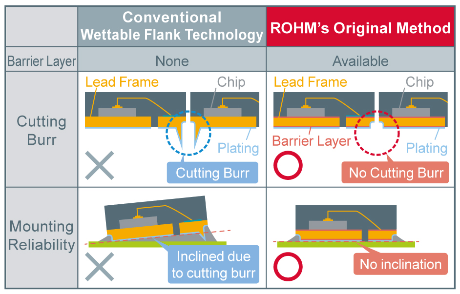 Figure 4: Comparison of wettable flank technologies
As a result, the RV4xxx series has been completely redesigned using wettable flank technology. The biggest difference from conventional products is that a material (barrier layer) with a hardness different from the lead frame is applied to the surface of the lead frame. This makes it possible to reduce burrs by approximately 50% over conventional methods.
Redesign for visibility
Reviewing construction methods resulted in the DFN1616, believed to be the first package to feature a guaranteed electrode height on the side of the package of 130μm by suppressing burrs. Currently, a toe fillet of 100μm may result in NG (no solder visible) during visual inspection, but the RV4xxx series is able to sufficiently clear the fillet height required by the automotive market (Figure 5).
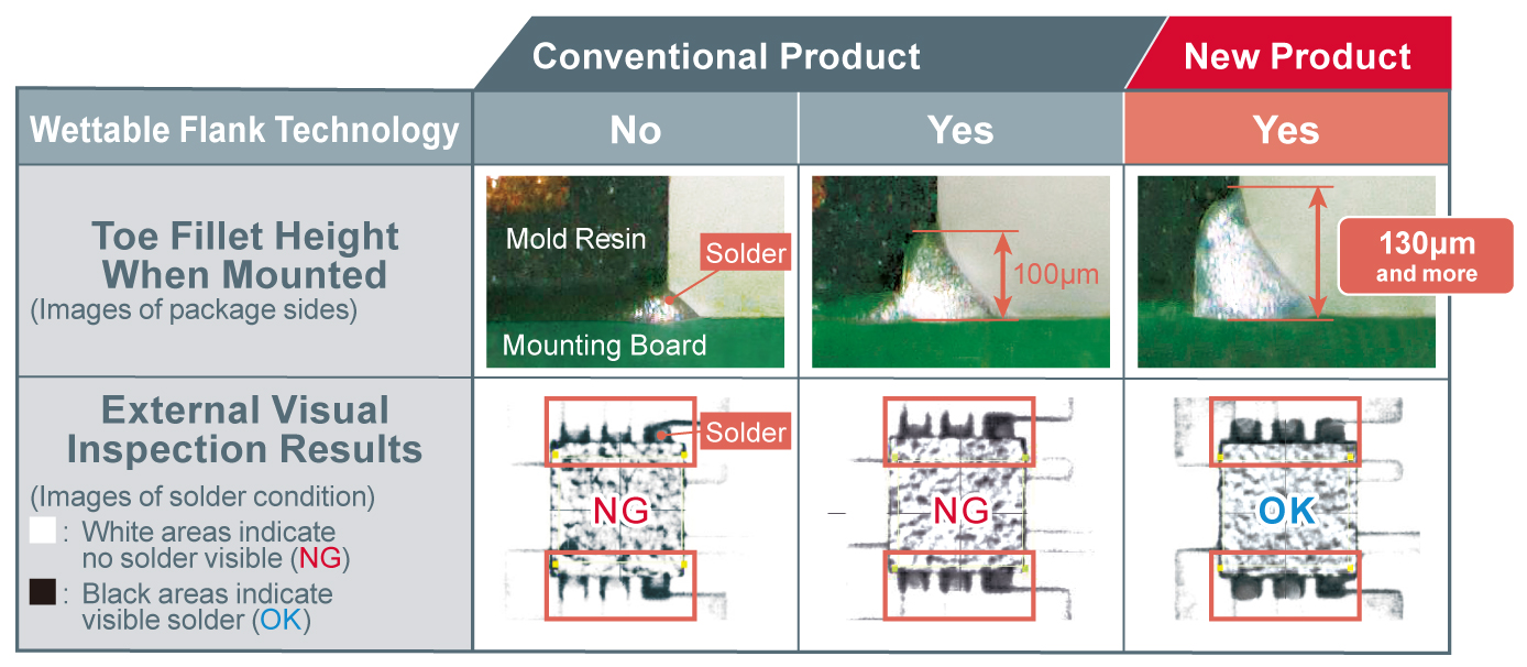
Figure 5: Mounting visibility comparison
Product Spotlight
TBF10SL-4PS-B
ITT Interconnect Solutions

| SKU: | 1003-TBF10SL-4PS-B-ND |
|---|---|
| Stock: | 50 |
| Cost: | $45.59 |
CAA572C0G3A663J640LJ
TDK Corporation

| SKU: | |
|---|---|
| Stock: | 1037 |
| Cost: | $9.16 |
RA1113112R
E-Switch, Inc.
| SKU: | EG5619-ND |
|---|---|
| Stock: | 5586 |
| Cost: | $0.55 |
R30-3002002
Harwin

| SKU: | 952-1510-ND |
|---|---|
| Stock: | 6545 |
| Cost: | $0.76 |
NRF54L15-QFAA-R
Nordic Semiconductor

| SKU: | 4823-NRF54L15-QFAA-RTR-ND |
|---|---|
| Stock: | 0 |
| Cost: | $2.39 |
STDRIVEG611Q
STMicroelectronics

| SKU: | 497-STDRIVEG611QTR-ND |
|---|---|
| Stock: | 0 |
| Cost: | $2.63 |
TBF10SL-4PS-B
ITT Interconnect Solutions
| SKU: | 1003-TBF10SL-4PS-B-ND |
|---|---|
| Stock: | 50 |
| Cost: | $45.59 |
CAA572C0G3A663J640LJ
TDK Corporation
| SKU: | |
|---|---|
| Stock: | 1037 |
| Cost: | $9.16 |
RA1113112R
E-Switch, Inc.
| SKU: | EG5619-ND |
|---|---|
| Stock: | 5586 |
| Cost: | $0.55 |
R30-3002002
Harwin
| SKU: | 952-1510-ND |
|---|---|
| Stock: | 6545 |
| Cost: | $0.76 |
NRF54L15-QFAA-R
Nordic Semiconductor
| SKU: | 4823-NRF54L15-QFAA-RTR-ND |
|---|---|
| Stock: | 0 |
| Cost: | $2.39 |
STDRIVEG611Q
STMicroelectronics
| SKU: | 497-STDRIVEG611QTR-ND |
|---|---|
| Stock: | 0 |
| Cost: | $2.63 |