


This article originally appeared in the Sept’23 magazine issue of Electronic Specifier Design – see ES’s Magazine Archives for more featured publications.
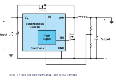
Automatic test equipment (ATE) requires four-quadrant operation for its device power supply (DPS) which can source and sink current while having positive or negative voltage. For higher current applications, multiple DPS can be used. Since the DPS can both sink and source current, the power supply for the DPS must have the same capability. The dual-output voltage rail reduces the number of bi-directional supplies needed to a single one, while still providing positive and negative bi-directional sources for the DPS. While many ICs are available that can source and sink current to make a bi-directional positive supply, the negative supply needs to source and sink current as well, as required by the device under test (DUT). A bi-directionally capable buck IC, for example, the LTC3871, can be configured to function as an inverting buck-boost converter (Figure 1).
How a converted buck IC works
When sourcing current, the inductor starts storing energy, ramping up the current while the output capacitor supplies the load. The inductor voltage is equal to the input voltage in this period.
When the control MOSFET is turned off, the sync MOSFET is turned on, and current flows through it. The output current is the average current of the sync MOSFET, and the inductor voltage is equal to the output voltage. As the inductor supplies the load and capacitor, its current starts to go down. This will repeat every switching cycle.
The feedback of the converter controls the pulse-width modulation (PWM) to regulate the output voltage to the desired level, which is set by the voltage divider resistors.
The output voltage is greater than the input voltage when the duty cycle is greater than 50% and less than the input voltage when the duty cycle is less than 50%.
When the converter starts sinking current, the current flows from the output to the input with a negative current flowing through the MOSFETs.
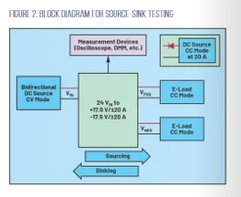
The-bi-directional DC source acts as the supply of the VPOS and is in CV mode. The other DC source is connected to the output of the VNEG. This DC source controls the amount of current that is sunk into the system. A blocking diode is connected in series with this DC source to ensure that no current will flow into it when the converter is sourcing current. The e-load is used as the initial load to show that the system is capable of transitioning from sourcing to sinking and vice versa.
When the DC supply is turned on, the VNEG rail starts to sink current. The inductor current waveform transitions from positive current to negative current. When the VNEG is sinking current, the system is open loop and the source-sink current is controlled by the CC mode of the external DC source. This is also true for the VPOS; when the DC source connected to its output is turned on, the VPOS rail starts to sink current.
Testing the transition
Waveforms in the source to sink transition show in the inductor current as it transitions from negative current to positive current. This indicates the transition back to sourcing current when the injected DC voltage across the VNEG is removed. This is also true for the VPOS rail.
The dual-output voltage rail reduces the equipment needed as it is already bi-directional capable on both the VPOS and VNEG. It is also more efficient as the current sunk on one rail is used to power the other rail, reducing the current that is sourced by the main supply. An additional benefit of the converter is that it allows for a greater selection of ICs to choose from when designing a bi-directional inverting buck-boost converter.