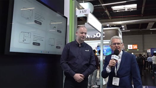
Denis Marcon General Manager, Europe, at Innoscience will take part in two forum discussions:
Power Electronic Forum, 11:50am, Wednesday November 16th, Stand A4.473: “How to take advantage of GaN power device performance.”
Markt&Technik Panel, 1:00pm, Wednesday November 16th, Stand C3.557 (WEKA): “Gallium Nitride – Beyond consumer electronics.”
Visitors to the Innoscience booth (C3.440) will be able to discuss with the team on the performance and applications of Low Voltage (30V-150V) GaN power devices such as the newly introduced JEDEC-qualified INN100W032A rated for 100V and featuring a low typical RDS(on) of just 2.4mΩ in a Solder Bar WLCSP package of just 3.5mm x 2.13mm package size. Innoscience will also show a demo of a 2.4kW, 48-12V bi-directional buck-boost converter for mild hybrid EVs (MHEV) and industrial applications based on the INN100W032A. Additionally, Innoscience will demonstrate a 150W Buck-Boost converter utilizing a 40V InnoGaN power device. This will demonstrate our solution size and performance benefits to power the next generation USB-C, PD3.1 designs for battery powered equipment and docking stations.
Moreover, Innoscience will showcase its bidirectional (BiGaN) power device that is the first GaN device to enter inside the mobile phone into the battery management system of the OPPO’s smartphone.
Next to this, Innoscience’s team will also present the High Voltage (650V) power GaN device portfolio with a wide range of on-resistances to satisfy a variety of power converter applications. Particularly, Innoscience will introduce the new JEDEC-qualified 650V GaN HEMT INN650D080BS with a typical RDS(on) of 60mΩ in a standard 8×8 DFN package. Such InnoGaNhas been used in the collaboration between Innoscience and KU Leuven/Energie Ville in Belgium to develop a 400V dual active bridge (DAB) converter with a power exceeding 1kW.
The same device has been used in another collaboration between Innoscience and BFH institute in Switzerland to realize a multi-level 800V converter.
Finally, Innoscience will present several demos that display the performance of its extensive range of High Voltage GaN HEMTs. Highlights will include a compact 300W PFC + LLC PD power supply based on the INN650D140A. Explains Innoscience’s Senior Business Development Manager, Christiam Gasparini: “This is a very compact and high efficiency platform for many products including consumer appliances through to industrial, computing, USB-C Power Delivery, medical and gaming, to name a few.”
Denis Marcon General Manager, Europe, at Innoscience commented: “We are excited to be at Electronica, the largest electronics event in the Western world, for the first time. We have both very competitive LV and HV GaN HEMTs available now in mass production and technical support teams in place to ensure that customers can take advantage of the benefits of GaN and leapfrog their competitors.”


