


Applications range from vehicle interiors and domestic appliances to medical devices and aircraft seating. Rather than relying on a mechanical or membrane switch, these surfaces utilise capacitive touch sensing – the same principle used in smartphone displays.
Capacitive sensing and backlighting of course require electronics behind the decorative exterior surface: in-mould electronics is an emerging manufacturing approach that promises to make functional surfaces cheaper, lighter, and more aesthetically pleasing.
What is in-mould electronics?
As the name suggests, in-mould electronics (IME) is a manufacturing method in which at least some of the electronics are subjected to a moulding process. Typically, this starts with screen printing the desired pattern of conductive ink onto a substrate (often polycarbonate) – these conductive patterns enable capacitive touch sensing. Next, a decorative layer is applied to the front, and the conductively patterned substrate is thermoformed to produce the required curvature. A subsequent injection moulding step is often applied. This approach of integrating electronics into the moulded part contrasts with conventional electronics manufacturing techniques, in which decorative user-facing parts would be moulded, and a printed circuit board (PCB) mounted onto the back afterward.
Why risk subjecting the electronics to this moulding process when a PCB behind a decorative surface would often suffice? Depending on the approach used, IME enables a weight and material consumption reduction of up to 70% relative to conventional mechanical switches. Furthermore, since fewer individual parts are required, both assembly and associated supply chains can be simpler. Given these advantages, along with growing engagement from both suppliers and integrators, IDTechEx forecast the market for IME parts that incorporates SMD (surface mount device) components to reach around $2 billion by 2033.
What are the competing approaches?
Within the umbrella term of ‘in-mould electronics’, there are many subtly different manufacturing approaches. Establishing which approach has been used is often tricky since the resulting functional surfaces look extremely similar. Two key variables are whether and at what point SMD components such as LEDs are mounted, and whether injection moulding is utilised.
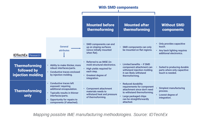
Arguably the most comprehensive approach to IME, developed by Tactotek and termed IMSE (in-mould structural electronics), involves mounting SMD components on a flat substrate prior to thermoforming. This is followed by injection moulding, embedding the components and conductive traces in plastic. The process results in a robust part with fully enclosed electronics, potentially including an integrated circuit.
A competing strategy is to mount the SMD components onto an already thermoformed part and neglect the injection moulding. This requires a thicker polymeric substrate to provide sufficient rigidity, which generally reduces the degree of distortion and curvature that can be introduced via thermoforming. Furthermore, SMD components can only be mounted via pick and place on regions that remain flat. However, for many applications, only slight curvature around the perimeter or in other specific locations is required, and since mounted components will not be subjected to the heat and pressure associated with moulding material specifications and design rules may be more forgiving.
The simplest approach to IME is to omit the SMD components altogether. Decorative surfaces with integrated capacitive touch can be produced relatively straightforwardly by first screen printing conductive ink then thermoforming the substrate. Subsequent injection moulding is optional. While these parts would require conventional electronics for backlighting, they represent an intermediate step between purely decorative and fully functional surfaces that can meet the needs of simpler use cases.
What does the future hold?
The wide variety of competing manufacturing approaches to in-mould electronics doesn’t imply a Darwinian scenario with only one winner – each approach offers a different balance of cost, form factor complexity, functionality, robustness, and size/weight reduction that can meet a particular need.
Overall, IDTechEx envisages a gradual trend towards greater functionality integration since it offers the most scope material and weight reduction but with greater adoption barriers than simpler manufacturing approaches.
How do i learn more?
IDTechEx’s new report, ‘In-Mould Electronics 2023-2033’, draws on over 20 company profiles, the majority based on interviews, to explore this emerging manufacturing methodology. This comprehensive report evaluates the technical processes, material requirements, and applications. It includes 10-year market forecasts by manufacturing methodology and application sector, expressed as both revenue and functional surface area.
Furthermore, the report provides a detailed evaluation of competing approaches, such as functional film bonding and the merits of including components such as LEDs within the IME parts.