


However, sometimes even these combined forces of innovation are not proving sufficient to meet the efficiency and power density demands of new paradigms such as vehicle electrification or burgeoning renewable energy applications. Printed circuit board (PCB) designers are increasingly coming to realise the importance of the role in which component packaging plays in enabling their designs to deliver on these requirements.
Researching and developing component packaging has always been at the heart of Nexperia activities and in this article, Frank Matschullat, Head of Product Group Power Bipolar, looks at some of the company’s historical achievements in this area before delving into how designers can overcome the challenges faced when adopting new developments – and what benefits this transition could have.
Nexperia’s history of innovating and developing semiconductor packaging
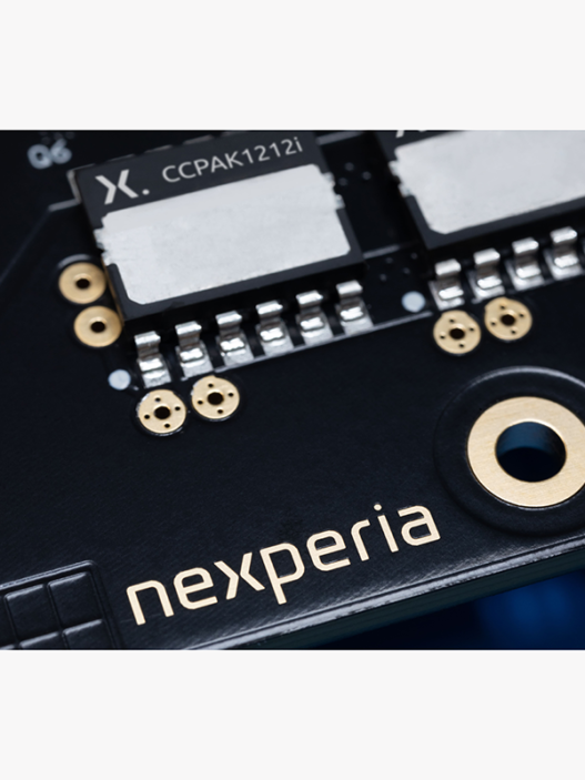
In April 1966 Piet van de Water at Philips (the company which would eventually beget Nexperia) began developing the 23rd Standard Outline Transistor (SOT23) package. Initial prototypes were released in 1968 before these innovative plastic encapsulated devices went into full production at our Hamburg site in 1969. From the 1980s, onwards the exploding popularity of consumer electronic devices saw surface-mount technology (SMT) begin to outpace through-hole boards and the SOT23 quickly became the de-facto standard three-pin surface mount package.While it has been ever present for more than half a century, Nexperia has not allowed the SOT23 to stand still – it developed a 5-pin variant, and the package is now produced lead-free (Pb). More recently, the operating temperature range for SOT23 packaged devices has increased to 175°C. The requirement for higher packaging power densities resulted in several spin-offs, including the SOT223 and SOT323. The need to improve efficiency and quality has also inspired Nexperia’s innovation in production methods and the types of equipment required to manufacture and assemble surface-mount devices (SMDs). In 2002, my colleague Ding Yandoc and our esteemed team here at Nexperia developed and pioneered a new concept that eliminated the requirement for wires to be bonded to the die. Instead, they used a large copper-clip attached to the source metallisation on the topside of the die to connect it to the outside. It also featured gull-wing pins that could efficiently conduct higher currents, while having sufficient flexibility to allow heat expansion and contraction without causing damage to the connection to either the die or board. Apart from increasing reliability, the new package, named LFPAK (loss-free package) also significantly reduced the thermal and electrical on-resistance of the device.
Dissipating heat more efficiently – from SOT23 to the copper-clip
Across most industries, the SOT23 surface-mount leaded package has traditionally been the most popular for transistors and diodes. The semiconductor die inside an SOT23 package is attached to a lead frame and typically has a direct connection to the source terminal while bond wires are used to attach the gate and drain leads. In contrast, DFN (discrete flat no-lead) devices feature two rows of closely spaced terminals on the underside of the package, which allows shorter bond wires to be used. These shorter bond wires improve electrical performance by reducing package inductance, thermal resistance, and die-free package resistance (DFPR). In a SOT23 package, internally generated heat conducts from the die-attached layer to the lead frame and onto the source lead before it reaches the substrate. On the other hand, in the latest DFN packages heat is conducted downwards to the source pad on the package underside. The shorter distance which the heat is required to travel makes power dissipation more efficient in DFN packaged devices. For many years, power diodes have also typically been housed in SMx packages, but these devices can carry significant amounts of current during switching transitions, meaning designers are looking to use packages which dissipate heat more efficiently. As a result, SMx packages are gradually being replaced by newer packages of the clip-bonded flatpower (CFP) type. CFP packages offer the dual advantage of reducing the amount of required PCB area by between 38 and 50% while also having superior heat dissipation properties when compared to a similarly rated SMx package. Using a copper clip, which enhances cooling from the die topside as well as the underside, as a replacement for bond wires was the key to achieving this improved thermal performance in loss-free packages like LFPAK, CCPAK as well as CFP. The top-side attachment has a much bigger surface area compared to an ordinary bond wire attachment and enables a much shorter heat dissipation pathway from die to the board. Furthermore, the large cross-sectional area of the clip means that heat is conducted to the underside of the package and into the substrate much more efficiently.
Package migration – obstacles and motivations
As with all innovation, these new technologies need to meet the cost-criteria set by customers. And while perception among some designers that newer style packages could potentially add to their board costs, there is a bigger picture to keep in mind. As modern electronic systems become more highly integrated, multi-layer PCBs are now often the only way to implement the complex wiring required to make them work. Faced with this already more expensive scenario, it can make sense for board designers to use CFP packaged devices, as their smaller footprint can help lower the overall system cost; a benefit that more than offsets the relatively small premium this packaging adds to the cost of individual devices. Furthermore, some CFP packaged devices can now be produced more cost-effectively than devices housed in older SMx and TO and DPAK packages. As with other legacy technology, over time, semiconductor manufacturers may begin to wind-down production of these device types, in favor of allocating more production capacity to newer devices. For this reason, it would be wise for designers to also begin thinking about migrating before supply bottlenecks for older package types become apparent and also to future-proof their products against the threat of obsolescence when longevity programs come to an end. With this history of package innovation under our belt, we want to encourage designers not to look at the features of components in isolation from the package in which they are sold. Instead, they should adopt a more holistic approach to literally see the complete ‘package’ i.e., look at the die function and how its housing can enhance (or inhibit) its performance. This approach also offers greater degrees of freedom in optimising the thermal performance of a design and its overall cost. For example, a slightly lower efficiency device in high performing packaging may be sufficient to meet design specifications than a higher efficiency device in a package with inferior thermal performance.
Conclusion
The perception that new semiconductor package options are ‘nice to haves’ for designers of premium electronic equipment is quickly disappearing as the merits and logic of their wider adoption become increasingly apparent. Indeed, the challenges of vehicle electrification and renewable energy equipment won’t be effectively overcome unless designers adopt a more holistic view of electronic components as a complete ‘package’. For these reasons, designers ignoring developments in the packaging sector do so at their peril. With Nexperia’s long-standing track record in researching and developing semiconductor packaging we are happy to share our expertise to help designers understand the challenges and benefits of making this transition.