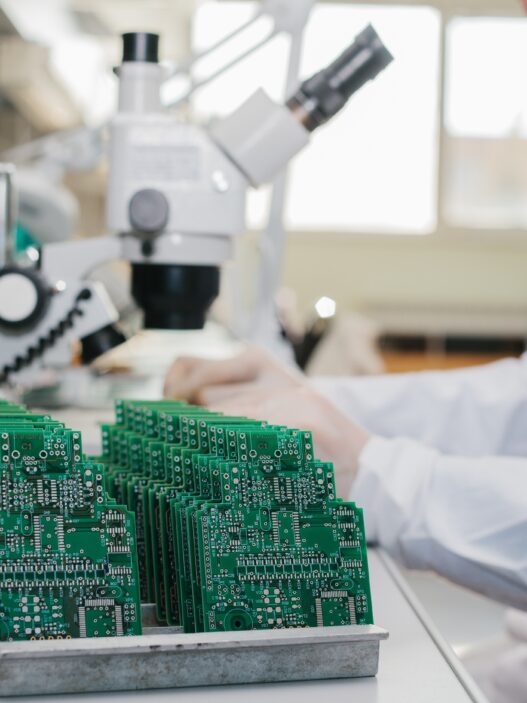


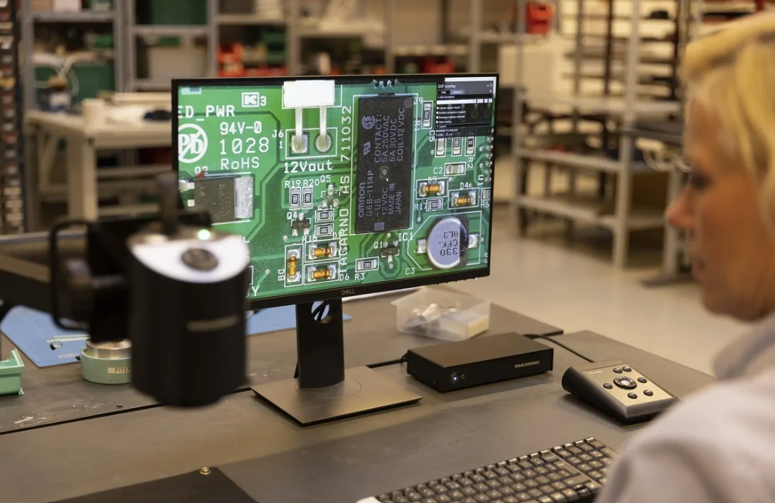
Magnification has been an integrated and crucial part of PCB production and rework for many years, and digital microscopes have taken PCB inspection to the next level.
What many electronics professionals find today is that traditional magnification systems can no longer provide the required magnification levels when doing quality control or when reworking faulty PCBs – nor are they equipped to capture photos and create documentation of your work in an efficient way. This sends PCB manufacturers hunting for new equipment that can do the job.
In this guide to digital microscopes within electronics, TAGARNO provides a detailed overview on:
- What to consider when choosing a digital microscope for soldering and PCB inspection
- The benefits of using a digital microscope for soldering and PCB inspection
- Different Electronics processes where you can use a digital microscope
- Choosing the best digital microscope for soldering and PCB inspection
TAGARNO’s line of microscopes offers a range of features and capabilities that make them ideal for a variety of applications. The company’s digital microscopes are designed to make it easier than ever to capture and share.
Read the guide here.