


This is driving fabricators to embrace new analytical techniques that can further their understanding of material structures, wafer processing, thin-film deposition, and interface preparation, in order to get the most out of existing silicon technologies.
This article takes a look at the vibrational spectroscopy solutions helping manufacturers to gain new material insights, bolster quality control, increase yields and reduce waste in order to maximise the notoriously wafer-thin profit margins involved in semiconductor production.
The quest for quality
Even minor faults or inconsistencies in the manufacturing process can significantly influence product yield, as well as affecting the function of final devices. For instance, metal shorts, opens, or transistor-level leakages can cause end-of-line test failures, with factors such as high density interconnects, wafer-level stacking, flexible electronics, and integral substrates making it increasingly difficult to detect these failure-inducing defects.
Implementing accurate, non-invasive inline monitoring technologies throughout the entire manufacturing workflow is therefore vital to identify issues early in the process, helping to shorten device development time, maximise yields, and ensure that semiconductor devices meet the evolving needs of the industry’s diverse customer base.
A spectrum of solutions
Semiconductor fabricators have employed vibrational spectroscopy techniques – such as Fourier-transform infrared (FTIR) spectroscopy and near infrared (NIR) spectroscopy – in quality control and R&D roles for several decades.
FTIR’s well-defined workflows and fit-for-purpose data reporting capabilities make it ideal for detecting silicon alloy defects during manufacture, as well as for rooting out impurities in the ultra-high purity gases used in many semiconductor processing operations. There has also been an increase in the use of FTIR spectroscopy during the development of new materials in recent years, allowing rapid determination of critical parameters such as bandgap width, lattice vibration, layer thickness and doping concentration.
NIR spectroscopy, on the other hand, can be used in combination with chemometric algorithms to monitor the concentrations of the multiple component solutions used in etching and cleaning, providing reliable in situ data that can be used to fine-tune processes and promote more efficient use of materials, while still maintaining high product yields. Additionally, non-invasive sampling via fibre optic cables allows remote placement of NIR instruments, as well as offering multi-point measurement capabilities.
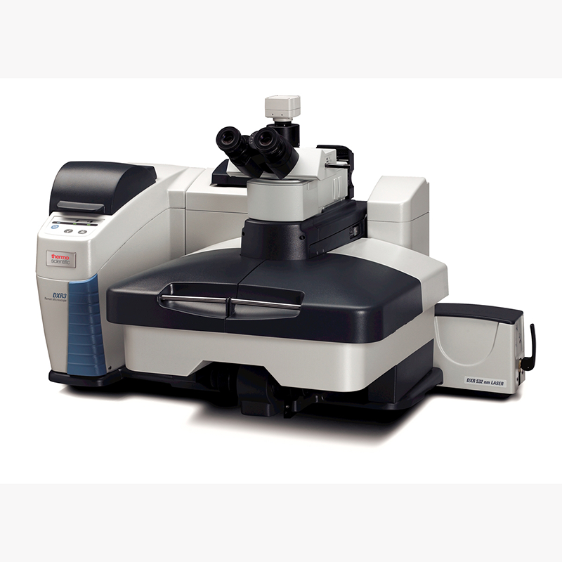
The rewards of Raman
Rapid diversification of the materials and methodologies used to produce semiconductor devices is also prompting manufacturers to include alternative metrology systems in the development process. Raman spectroscopy, for example, is ideally suited to the characterisation of a wide range of novel silicon, carbon-based and group III-V alloys – as well as polymers – due to the distinct Raman bands exhibited by these materials. This versatile technique can provide a wealth of information about chemical composition, polytype, stress and strain profiles, dopant concentration, crystal structure type, and purity. Recent advances in Raman microscopy have also led to sub-micron resolution imaging capabilities, prompting many fabricators to promote Raman spectroscopy to be a mainstay of their metrology toolboxes.
Streamlining with spectroscopy
Increasingly demanding device designs are making the margin for error in semiconductor development and fabrication tighter than ever, and manufacturers must be sure to employ cutting-edge techniques that can root out inefficiencies and inconsistencies wherever they lie.
The combination of modern FTIR, NIR, and Raman spectroscopy can offer the perfect blend of accuracy and versatility to help streamline the entire semiconductor operation – from material development to manufacturing quality control – giving semiconductor fabricators the tools they need to thrive in such a rapidly evolving market.