


Silicon has been the dominant semiconductor material of choice for decades. However, research into other compound semiconductor materials, specifically silicon carbide (SiC) and gallium nitride (GaN), has reinvigorated power conversion and motor drive applications with more efficient, smaller, and robust semiconductor devices that bring significant performance benefits.
In semiconductor physics, a bandgap is an energy range in a solid between a valence band and a conduction band where no electrical states exist. Crossing the gap requires an electron to possess sufficient energy, measured in electron volts (eV), to achieve conduction and create a current flow. Materials with relatively low bandgap attributes are typically semiconductors, and those with a high bandgap are insulators.
For example, silicon has a bandgap characteristic of 1.1eV, while gallium nitride and silicon carbide have similar bandgap values in the range of 3.2eV to 3.4eV. With a bandgap three times that of silicon, power semiconductors such as MOSFETs and JFETs fabricated from these compound materials are more suited to high voltage applications such as motor gate drives and switching circuits. High bandgap values also result in lower leakage currents, and a high electron saturation velocity metric permits operation at high switching frequencies.
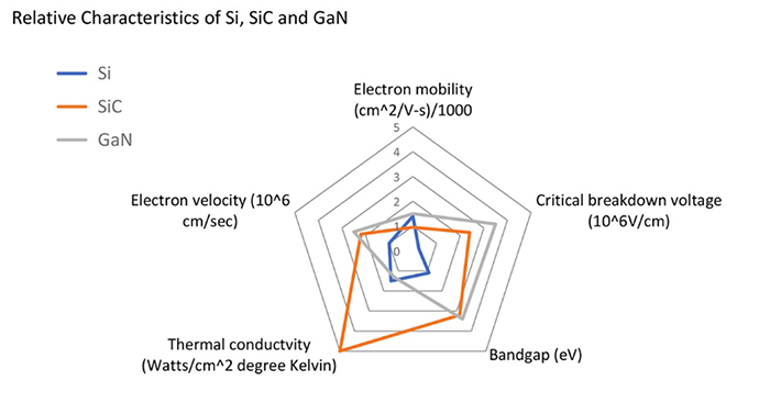
Above: Comparing the electrical and physical properties of silicon carbide and gallium nitride wide bandgap materials compared to silicon (Source: Mouser)
Other electrical differences between silicon and WBG materials (silicon carbide and gallium nitride) include a significantly higher dielectric breakdown voltage and a high degree of electron mobility. Silicon’s breakdown voltage is approximately 0.3MV/cm compared to SiC’s 3.5MV/cm and GaN’s 3.3MV/cm, illustrating that wide bandgap devices exhibit a breakdown voltage characteristic at least a factor of ten better than silicon.
The electron mobility, a factor that indicates how quickly electrons can move through the compound semiconductor, highlights differences between SiC and GaN and the applications they suit. GaN exhibits electron mobility of 2,000cm^2/Vs compared with silicon’s 1,500cm^2/Vs. However, SiC has much slower electron mobility, approaching 650cm^2/Vs, making them less suitable for high-speed switching applications. GaN, however, with its three times faster electron mobility compared to SiC, suits operation at higher switching frequencies.
Technical advantages of wide bandgap devices
Thermal conductivity is another physical characteristic that impacts high power conversion and motor drive applications. The heat generated within the device needs to be conducted away as efficiently as possible. The thermal conductivity metric highlights how efficient a material is at conducting heat through itself. This time gallium nitride’s thermal conductivity ability is slightly less than silicon, but silicon carbide’s thermal conduction efficiency is three times better, making it ideal for high-temperature applications.
Another vital characteristic of wide bandgap compound semiconductors is that their conduction resistance Rds(on) is significantly less than silicon-based MOSFETs, reducing substantial switching losses experienced in power conversion applications. Other fractional switching losses occur in the associated passive components used within power converters such as inductors, transformers, and capacitors.
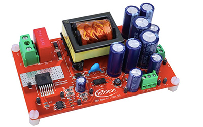
Above: The Infineon REF_62W_FLY_1700V_SiC reference board featuring a 1,700V Infineon CoolSiC MOSFET (Source: Infineon)
Also, the physical construction of SiC and GaN devices is smaller and weighs less than their silicon counterparts allowing for more compact and lightweight semiconductors. With smaller die sizes, the impact of device internal capacitances reduces, allowing faster switching frequencies. For example, a silicon-based MOSFET has a die area approximately five times larger than a SiC-based MOSFET for the same operating voltage range.
With the benefits highlighted above, wide bandgap semiconductor devices are ideal for power conversion and motor drive applications. The advantages are inter-related and together contribute to more energy efficient, compact, and robust end-applications. The differences between gallium nitride and silicon carbide also dictate which WBG material is suitable for a particular application. For example, with its superior thermal conductivity, SiC is suited for use in high temperature systems.
The ability to use higher switching frequencies with GaN and SiC-based circuits leads to smaller inductors and capacitance values, further saving PCB space and bill of material (BOM) cost.
Wide bandgap power conversion in practice
Wide bandgap devices are now readily available in various package sizes, process technologies, and voltage ratings from multiple suppliers, including Infineon, STMicro, and Rohm. In addition to the devices themselves, evaluation boards and reference designs help speed prototyping and developing an end-product. Infineon offers both SiC and GaN devices with their CoolSiC and CoolGaN product portfolios.
An example CoolSiC device is the 1,700V SiC Trench MOSFET. Optimised for use in flyback converter topologies, it has very low switching losses and is compatible with most 12V controller driver ICs. The MOSFET is packaged in a TO-263 7L surface mounted format, and the creepage distance between drain and source is seven millimetres, ensuring the end-product safety standard can be readily met. Also, a separate driver source pin helps reduce gate ringing typically caused by the parasitic inductance of the gate loop.
The above Infineon CoolSiC MOSFET features in the reference board REF_62_FLY_1700_SiC, which aids engineers wishing to develop an auxiliary power supply using a three-phase single-ended flyback converter topology – see Figure 2.
In typical operation, the reference board operates in a quasi-resonant mode (QRM) to keep the impact of EMI noise to a minimum. When operating with loads more than 30% of full power, the converter can optionally switch to using discontinuous conduction mode (DCM) for which the maximum operating frequency is set to 130kHz. The board delivers three nominal output voltages of +15V, -15V, and +24V.
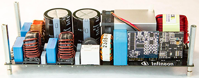
Above. The Infineon CoolGaN 2,500W full-bridge totem-pole PFC AC/DC converter demonstration board (Source: Infineon)
Additional features of the reference board include an adjustable output over-voltage protection, current overload protection, auto restart from over-temperature conditions, and Vin over- and under-voltage protection.
Infineon’s CoolGaN product line-up includes a 600V enhancement-mode, usually off ultra-fast switching power transistor, the IGOT60R070D1.
The device has a maximum Rds(on) rating of 70mΩ and suits use in high-frequency half-bridge totem-pole power factor correction (PFC) circuits. With low gate charge and low output charge characteristics, the transistor is ideal for industrial, telecommunications and data centre applications.
A 2,500W full-bridge totem-pole PFC demonstration board – see Figure 3 – using the CoolGaN IGOT60R070D1 device, highlights the benefits of using GaN technology to achieve a conversion energy efficiency as high as 99.2% in efficiency critical applications. A totem-pole PFC uses semiconductor switches instead of a bridge rectifier or individual diodes to create a highly efficient AC/DC converter circuit. The control circuit uses a constant PWM switching frequency of 65kHz and a continuous conduction mode controller IC.
STMicroelectronics’ line-up includes 650V and 1,200V silicon carbide MOSFETs – see Figure 4. Product examples include the SCTW70N120G2V and the SCTW100N65G.
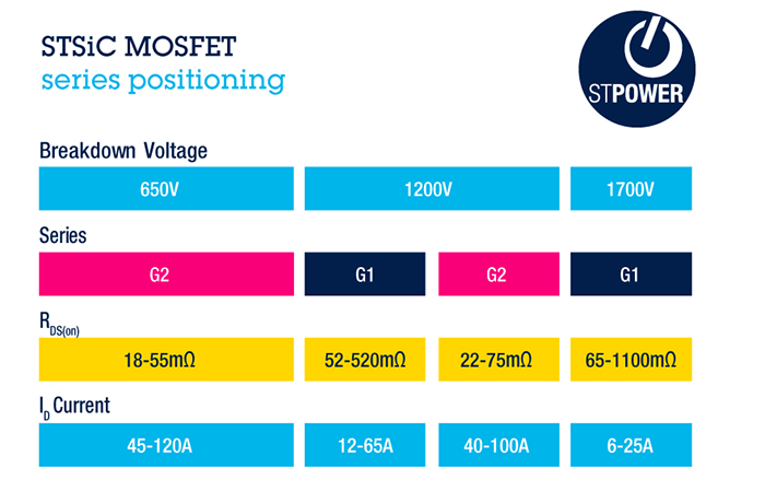
Above: The STMicroelectronics portfolio of silicon carbide MOSFETS (Source: STMicroelectronics)
The SCTW70N120G2V is a 1,200V device constructed in a HiP247 package, has a Rds(on) of 21mΩ, and can sustain a maximum drain current of 91A. The MOSFET incorporates a fast and robust body diode and has low gate charge and input capacitances. It is suitable for a variety of DC/DC conversion, charger, and renewable energy system applications.
Another SiC MOSFET is the SCTW100N65G, an automotive-grade AEC-Q101 qualified 650V, 100A semiconductor with a Rds(on) of 20mΩ. Both these STMicroelectronics MOSFETs are suitable for high-temperature applications with a 200°C junction temperature capability.
ROHM Semiconductor offers high power silicon carbide MOSFETs such as the SCT3033KLGC11. This 1,200V, 95A device has a Rds(on) of 22mΩ and a maximum junction operating temperature of 175°C. Applications include a broad range of power conversion, solar power inverters, and motor control designs.
A final product example comes from GaN Systems with its GS6100x series of 100V GaN enhancement transistors. Using a bottom-side cooling method, the GS61004B device has an Ids(max) of 38A, a low Rds(on) of 18mΩ, and accommodates high switching frequencies greater than 10MHz. An evaluation board, GS61004B-EVB-CD, incorporates two GS61004B transistors in a full-bridge.
Conclusion
Wide bandgap semiconductors herald new energy efficiency levels, higher switching frequencies, and operating temperatures for motor gate drive and power conversion circuits. Silicon carbide and gallium-nitride MOSFETs and transistors, together with complementary design resources, are now readily available for engineers to incorporate in next-generation designs.