


One critical consideration when implementing inference accelerators (or for that matter, hardware accelerators in general) relates to how we access memory. In the context of machine learning (ML) inference, we specifically need to consider how we store both weights as well as the intermediate activation values. For the last few years, several techniques have been used with varying degrees of success. The impacts of the related architectural choices are significant:
Latency: Access to L1, L2, and L3 memory exhibits relatively low latency. If the weights and activations associated with the next graph operation are cached, we can maintain reasonable levels of efficiency. However, if we need to fetch from external DDR, there will be a pipeline stall, with the expected impacts on latency and efficiency.
Power consumption: The energy cost of accessing external memory is at least one order of magnitude higher than accesses to internal memory.
Compute saturation: In general, applications are either compute-bound or memory-bound. This may impact GOP/TOPs achievable in a given inference paradigm, and in some cases, this impact may be very significant. There is less value in an inference engine that can achieve 10 TOPs peak performance if the real world performance when deploying your specific network is 1 TOP.
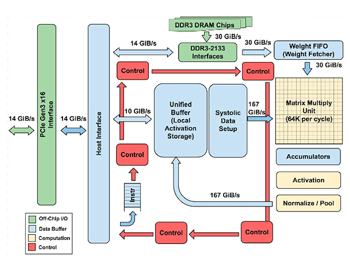
Above: Figure 1. TPUv1 architecture
To take this one step further, consider that the energy cost of accessing internal SRAM (known as BRAM or UltraRAM to those familiar with Xilinx SoCs) in a modern Xilinx device, is in the order of picojoules, roughly two orders of magnitude less than the energy cost of accessing external DRAM.
As one architectural example, we can consider the TPUv1. The TPUv1 incorporated a 65,536 INT8 MAC unit together with 28MB of on-chip memory to store intermediate activations. Weights are fetched from external DDR. The theoretical peak performance of TPUv1 was 92 TOPS.
The TPU is one example of a very generalised Tensor accelerator that uses a complex compiler to schedule graph operations. The TPU exhibited very good efficiency throughput for specific workloads (reference CNN0 at 86 TOPS). However, the ratio for computation over memory reference for CNNs is lower than for MLPs and LSTMs, and we can see that these specific workloads are memory bound. CNN1 also performs poorly (14.1 TOPS) as a direct result of the pipeline stalls that occur when new weights must be loaded into the matrix unit.
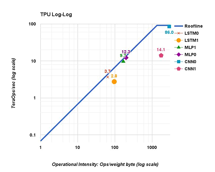
Above: Figure 2. TPUv1 performance roofline for various network topologies
Neural network architecture has a significant impact on performance, and the peak performance metric is of little value in the context of selecting an inference solution unless we can achieve high levels of efficiency for the specific workloads that we need to accelerate. Today, many SoC, ASSP and GPU vendors continue to promote performance benchmarks for classical image classification models such as LeNet, AlexNet, VGG, GoogLeNet, and ResNet. However, the number of real world use cases for the image classification task is limited, and many times such models are only employed as a back-end feature extractor for more complex tasks such as object detection and segmentation.
More realistic examples of real world deployable models are object detection and segmentation. How does this correlate with the observation that you have to look long and hard to find official IPS benchmarks for networks such as YOLOv3 and SSD, despite many semiconductor devices being marketed as offering 10s of TOPs of performance?
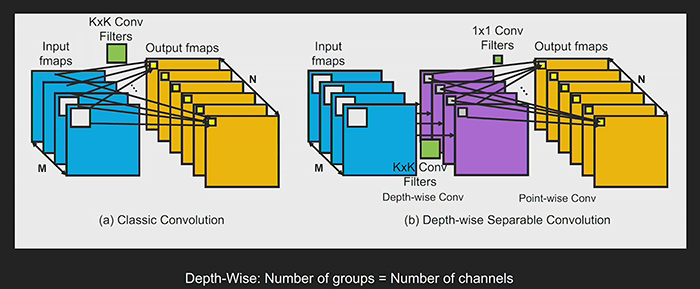
Above: Figure 4. classical versus depth-wise convolution connectivity
Is it any wonder that many developers find that their first ‘kick’ at designing an AI-enabled product fails to meet performance requirements, forcing them to migrate to a different architecture mid-design. This is particularly challenging if it means re-architecting both SOM base-board hardware and software. It turns out that a key motivator for selection of Xilinx SoCs is that the company’s inference solutions scale directly by more than an order of magnitude in performance, while maintaining the same processor and same inference accelerator architectures.
In 2017, a team of researchers from Google (Howard et al, ‘MobileNets: Efficient Convolutional Neural Networks for Mobile Vision Applications’) presented a new class of models targeted to mobile applications. MobileNet’s advantage was that it considerably reduced computational cost while maintaining high levels of accuracy. One of the key innovations employed in MobileNet networks is separable depth-wise convolution. In the context of classical convolution, every input channel has an impact on every output channel. If we have 100 input channels and 100 output channels, there are 100×100 virtual paths. However, for depth-wise convolution, the convolution layer is split into 100 groups with the result that there are only 100 paths. Each input channel is only connected with one output channel, with the result that a lot of computation is saved.
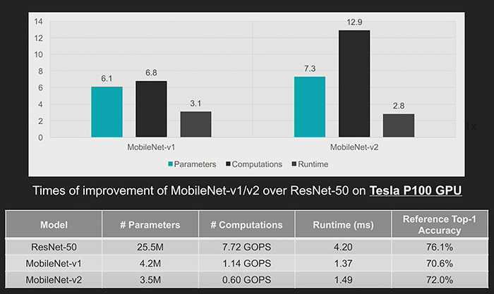
Above: Figure 5. MobileNet vs ResNet50 Ops and Latency
One result of this is that for MobileNets the ratio of computation to memory is reduced, with the implication that memory bandwidth and latency plays a more important role in achieving high throughput.
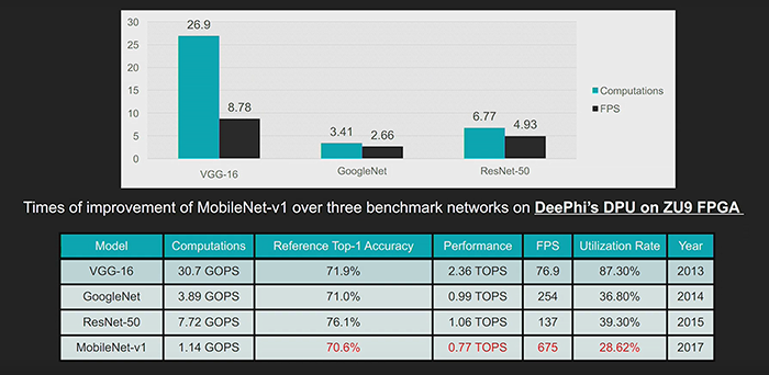
Unfortunately, computationally efficient networks are not necessarily hardware friendly. Ideally, latency would scale down in linear proportion to the reduction in FLOPs. However, as they say, there’s no such thing as a free lunch. Consider for instance the comparison in Figure 5 which shows that the computational workload for MobileNetv2 is less than one-tenth the workload for ResNet50. However, latency does not follow the same trajectory.
In Figure 5, we can see that the latency does not scale down by 12x in proportion to the reduction in FLOPs.
So how do we solve this problem? If we compare the ratio of off-chip communication over computation, we see that MobileNet has a very different profile than VGG. In the case of the DWC layers, we can see that the ratio is 0.11. The accelerator is now memory bound and thus achieves lower levels of efficiency as many elements of the PE array sit like ‘dark’ servers in a data centre, consuming power and die area, while performing no useful work.
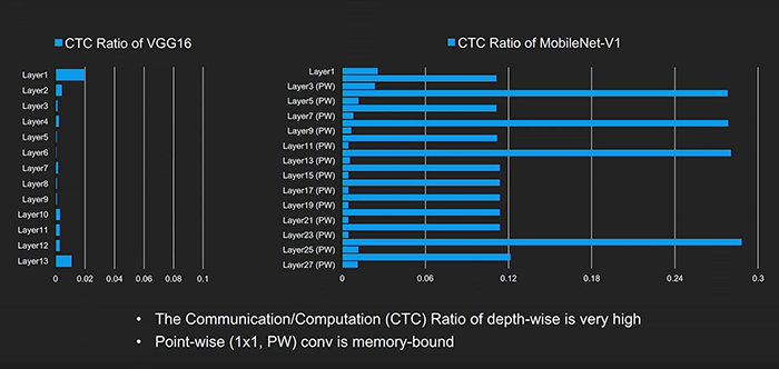
Above: Figure 6. CTC Ratio of VGG16 and MobileNetv1
When Xilinx released the DPUv1, it was designed to accelerate (among other ops) conventional convolution. Conventional convolution requires a channel-wise reduction for the input. This reduction is more optimal for hardware inference because it increases the ratio of compute to weight/activation storage. Considering the energy cost of compute versus memory, this is a very good thing. This is one of the reasons that deployments of ResNet-based networks are so prevalent in high performance applications – the ratio of computation to memory is higher with ResNet than it is with many historic backbones.
Depth-wise convolutions do not result in such channel-wise reductions. Memory performance becomes much more important.
For inference, we typically fuse the DWC with the PWC convolution and store the DWC activations in on-chip memory and then start the 1×1 PWC immediately. In the context of the original DPU, there was no specialised hardware support for DWCs, with the result that the efficiency was less than ideal.
To accelerate the performance of DWC in hardware, Xilinx modified the functionality of the PEs (processing elements) in the Xilinx DPU, and fused the DWC operator with the point-wise CONV. After one output pixel is processed in the first layer, the activation is immediately pipelined to the 1×1 convolution (through on-chip BRAM memory in the DPU) without writing to DRAM. We can greatly increase the efficiency of MobileNet deployments on the DPU using this specialised technique.
Above: Figure 7. MobileNet vs ResNet50 Ops & Latency – DPUv1 (no native DWC support)
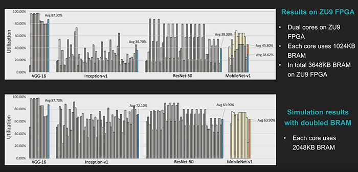
With this modified DPUv2 architecture Xilinx are able to deliver a dramatic improvement in the efficiency of MNv1 inference. Furthermore, by increasing the amount of on-chip memory, the company can further increase the efficiency such that it is on-par with its ResNet50 results. All of this was accomplished using the same CPU and hardware architecture.
A common occurrence is to optimise the inference hardware and neural network model in isolation from each other. Networks are generally trained using GPUs, and deployed at the Edge on SoCs, or GPUs with a dramatically different architecture. To truly optimise performance, we must adapt hardware to efficiently deploy models which are not necessarily hardware friendly. The key advantage of adaptable hardware in this context is that Xilinx devices offer an opportunity to continue to co-evolve both software and hardware post tape-out.
To take this one step further, consider the implications of this ground-breaking paper, entitled ‘The Lottery Ticket Hypothesis’ (Frankle & Carbin, 2019). In this paper (one of two that proudly wore the crown at ICLR2019) the authors ‘articulate the hypothesis’ that ‘dense, randomly-initialised, feed-forward networks contain subnetworks (winning tickets) that – when trained in isolation – reach test accuracy comparable to the original network in a similar number of (training) iterations’. It is clear then that the future for network pruning remains bright, and techniques such as AutoML will soon illuminate ‘winning tickets’ for us as part of the network discovery and optimisation process.
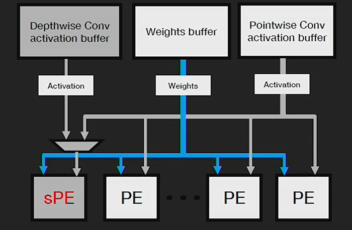
Above: Figure 8. DPUv2, specialised DWC processing element
It is also true that the best solution today to ensure efficient and high-accuracy deployments at the edge, remains channel pruning of classical backbones. While these backbones may be inefficient for deployment, semi-automated channel pruning of such backbones can deliver extremely efficient results (reference the Xilinx VGG-SSD example). It’s quite probable that the ‘winning ticket’ can today be found simply by selecting an inference architecture that will future-proof your next design, enabling you to take advantage of future network architectures and optimisation techniques while ensuring product longevity for your customers.
Above: Figure 9. MobileNet vs ResNet50 Deployment Latency, DPUv1 versus DPUv2 (DWC support)
There are numerous possibilities that will abound as future research derived from ‘The Lottery Ticket Hypothesis’ leads us to a new generation of pruning techniques for even greater efficiency gains. Furthermore, it is more than just intuition that tells us that only adaptable hardware, offering multi-dimension scalability, will provide a vehicle for you to collect the prize.
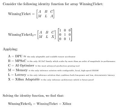
Above: Figure 10. Quenton Hall’s personal ‘Winning Ticket’ hypothesis