


Traditional designs for industrial data acquisition often require elaborate filtering on the analogue front end (AFE) in front of the analogue-to-digital converter (ADC). An analogue filter’s primary objective is to attenuate unwanted out-of-band signals that can alias on top of the desired signal of interest – so the analogue filter is also known as an anti-alias filter (AAF). Unwanted signals and noise in the alias band can originate from the driving amplifier, power supply switching spurs or even intentional interferers (jammers).
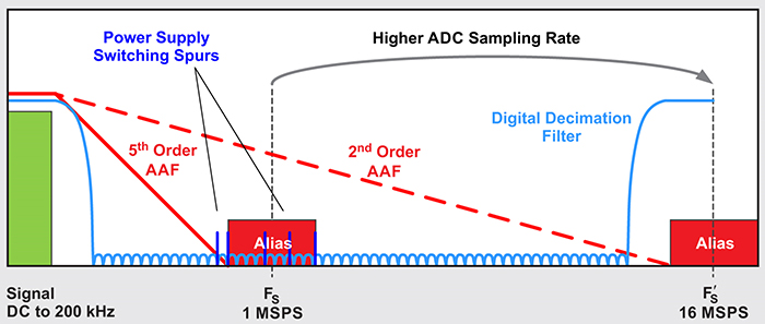
Above: Figure 1. Anti-alias filter relaxation due to increased ADC sampling rates
The alias frequency location directly depends on the ADC sampling rate – the faster the data converter can operate for a given instantaneous bandwidth, the further away the alias band gets from the desired signal, and the easier filtering becomes. In very high precision systems, designers often exploit this relationship by using deltasigma ADCs – which by design use high oversampling rates along with decimation filters. In cellphone base stations, the push for direct radio-frequency sampling of the 3GPP bands from 1-6GHz drove the adoption of gigasample-per-second (GSPS) data converters. The instantaneous bandwidth of the 3GPP bands are only a fraction of the sampling rate, thus the new architecture of using oversampling GSPS converters also relaxed the requirements for the analogue RF filter.
Industrial applications using successive approximation register (SAR) ADCs – such as power quality analysis, sonar or industrial radar with sampling rates between 1 MSPS to more than 10 MSPS – fall in between precision delta-sigma and GSPS ADC. The new ADC35xx and ADC36xx families of high-speed SAR ADCs are coupled with an integrated digital filter, enabling industrial applications to take advantage of this oversampling and decimation design technique in order to relax external analogue filter requirements.
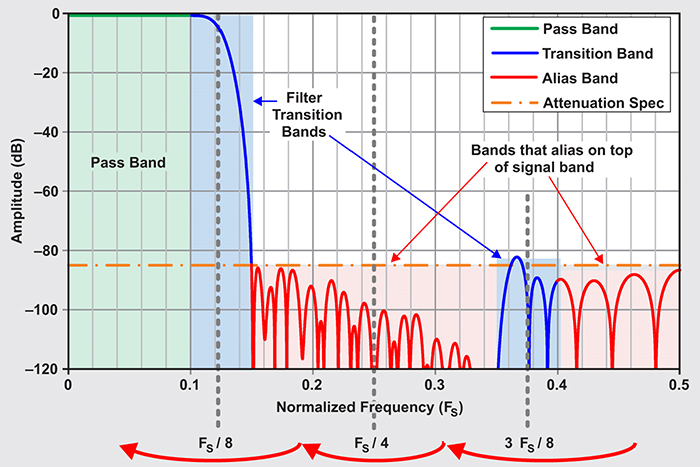
Above: Figure 2. Decimation filter regions in the frequency domain
For the example shown in Figure 1, assume that the DC input signal is 200kHz with an ADC sampling rate of 1 MSPS. A passband of around 300kHz together with an alias rejection of around 40dB requires approximately a fifth order filter. By increasing the ADC sampling rate from 1 MSPS to 16 MSPS, the alias frequency band gets pushed out from 800kHz to 15.8MHz and therefore reduces the anti-alias filter to a second-order filter. Additionally, the alias band shifts away from the frequency region (600kHz to 2MHz), which often contains spurs from switching regulators in the power supply.
Internal digital filter
The next objective is to examine the three purposes of the internal digital filter.
- Attenuation of the alias frequency band: The most common digital decimation filter in the frequency domain is a digital low-pass filter. This filter consists of three different regions: the passband, the multiple transition bands and the alias bands, as shown in Figure 2. Any signals in the alias bands will alias on top of the passband but will be attenuated by around 85dB or more in this figure. All three alias bands mirror around FS/8, FS/4 and 3 FS/8.
- Output data-rate reduction: A high oversampling rate can be hard to handle for downstream processors. Furthermore, in an oversampling configuration, most of the frequency spectrum only contains unwanted content, which expends unnecessary energy to transmit. The digital filter discards samples and reduces the output data rate.
When the band of interest is not in the low-end frequency range, a digital mixer can down convert the signal before low-pass filtering in order to maximise the reduction in output rate. - SNR improvement: The signal-to-noise ratio (SNR) of a data converter is calculated by integrating the noise floor across the ADC’s Nyquist zone. In theory, the ADC SNR improves by 3dB for every factor of 2 digital decimation. In reality, it is possible to get close to 3dB until in-band noise starts to dominate.
In the earlier example, the ADC sampling rate increased from 1 MSPS to 16 MSPS. Adding a decimate by 16 digital filter would reduce the output rate back to 1 MSPS while increasing the ADC SNR by as much as 12dB (4×3dB).
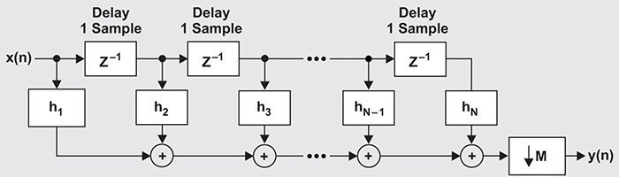
Above: Figure 3. Implementation example of a FIR design
Noise spectral density (NSD) is another measure of data-converter noise performance. It takes the SNR and bandwidth into consideration and is often used to compare different data converters. For example, a 16-MSPS ADC with an SNR of 82dB would have an NSD of –151dBFS/Hz [82dB + 10 × LOG (8MHz)]. After decimation by a factor of 16, the SNR improves by 12dB (from 82 to 94dB), while the NSD stays constant at –151 dBFS/Hz [94dB +10 × LOG (0.5MHz)].
Understanding the decimation filter
Several trade-offs determine the architecture of the digital filter and the number of filter taps: programmable vs. fixed coefficients, the maximum passband ripple, the minimum stop-band attenuation, latency and power consumption. For example, a sharper filter roll-off and more stop-band attenuation require a higher number of filter taps, resulting in higher power consumption and longer latency. The filter coefficients determine whether the filter gives a lowpass, high-pass or band-pass frequency response.
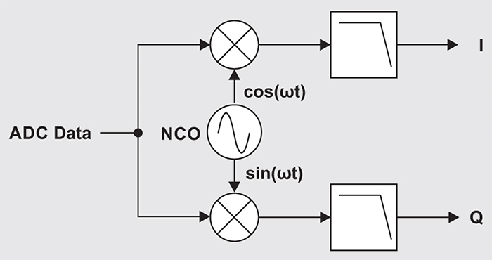
Above: Figure 4. Block diagram of a complex decimation filter
When integrating a digital filter with a high-speed data converter, a finite impulse response (FIR) half-band lowpass filter is most commonly used by ADC designers because its design is inherently very power efficient. Half band means decimation by 2; every other coefficient is zero, and these coefficients don’t use any computational power. Non-zero coefficients are symmetrical around the centre of the impulse response.
Figure 3 shows a generic FIR implementation. In a half-band implementation with seven taps/coefficients (N = 7), all even taps (h2, h6) except h4 are zero, which reduces seven multiplications to five. For higher decimation rates, halfband filters are concatenated.
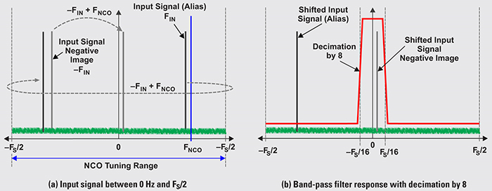
Above: Figure 5. Illustration of complex filtering
In theory, a low-, high- or band-pass filter could be integrated with the ADC. However, a low-pass filter is the most practical choice, especially when adding a complex mixer to build a digital tuner.
Note that the digital filter sits after the analogue-to-digital conversion. Therefore, the digital filter can’t prevent intended or unintended jamming of the receiver where the ADC gets driven into saturation. It is important to still use external filtering and adjustable gain to prevent overloading of the ADC.
Complex decimation-digital tuner
Adding a complex mixer [using cos(ωt) and sin(ωt) for I/Q output] turns the two digital low-pass filters into a tunable digital band-pass filter as can be seen in Figure 4. The mixer uses a numerically controlled oscillator (NCO) as the local oscillator (LO). Both the ‘I’ path and the ‘Q’ path are real low-pass filters in the frequency domain. The phase difference between sine and cosine cancels the positive/negative frequencies. The digital mixer shifts any frequency within the positive or negative Nyquist zone to zero Hertz, thus creating a very powerful tunable bandpass filter – while also replacing a traditional analogue mixer.
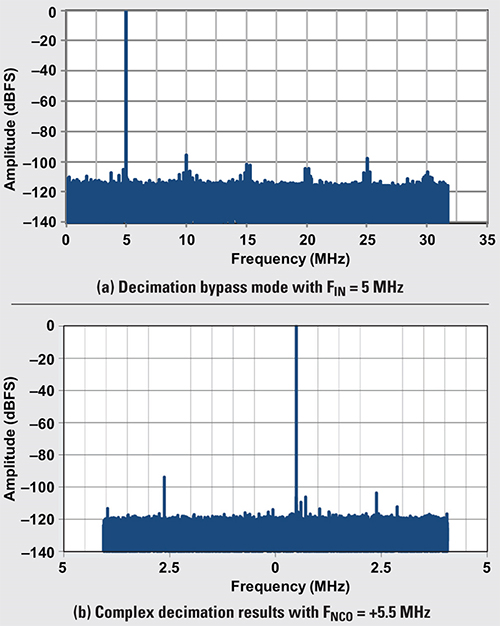
Above: Figure 6. Performance example of integrated decimation filter with FS = 65 MSPS
Figure 5 illustrates the process of digital tuning. The Nyquist zone of the ADC shows the input signal (FIN) between 0Hz and +FS / 2. The negative image of that input signal (–FIN) is located between 0Hz and –FS / 2. Both the input signal and its negative image are mixed with the NCO frequency (+FNCO in this example). +FIN rotates to the negative Nyquist zone while –FIN rotates to the positive Nyquist zone. The example shows a band-pass filter response with decimation by 8 cantered at 0Hz, which passes the –FIN frequency mixed with the NCO frequency (FOUT = –FIN + FNCO).
Practical examples
In time-domain applications, a digital low-pass filter can remove higher-frequency noise on the input signal. When sampling a pulse-shaped waveform, the low-pass filter will remove higher-order harmonics, thus slowing down the edge rate of the pulse.
In frequency-domain applications such as radar, the integrated decimation filter becomes a very powerful feature for the reasons outlined earlier in this article. Further illustrated in Figure 6, the input signal FIN is sampled with FS = 65 MSPS, followed by complex decimation by 8 and an NCO frequency of 5.5MHz.
Conclusion
In an effort to reduce the size of the printed circuit board and bill-of-materials cost, designers are looking to replace analogue circuits with digital logic/ intellectual property (IP). High-speed SAR data converters with integrated digital filtering like those in the ADC35xx and ADC36xx families are a good fit for a wide range of industrial applications. Similar to a delta-sigma converter, these ADCs ease analogue filter constraints with a higher oversampling rate combined with integrated digital filtering. The complex mixer can also remove an analogue mixing stage, further simplifying the analogue front end signal chain.