


This article originally appeared in the Oct’23 magazine issue of Electronic Specifier Design – see ES’s Magazine Archives for more featured publications.
The increased popularity of EVs means energy that has been distributed as gasoline will be replaced by electricity, raising the importance and spread of charging stations.
EV charge stations can be classified into three types. These are AC Level 1 – residential chargers, AC Level 2 – public chargers and the third is DC fast chargers. Yole Group’s forecast (Figure 1) predicts that the DC charger market will grow at a CAGR of 15.6% between 2020 to 2026.
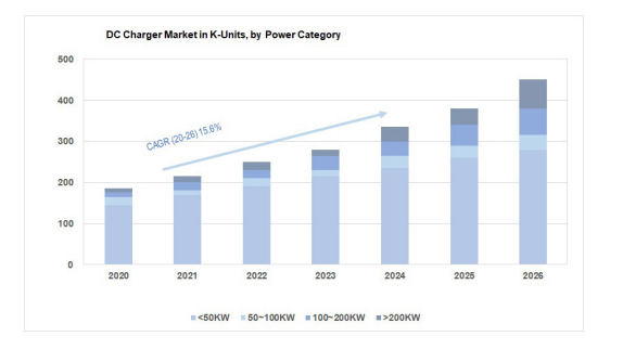 Figure 1. DC charging for plug-in EVs, 2021 (Source: Yole Group).
Typically, there are two types of charging technologies which are V2H (vehicle to home) and V2G (vehicle to grid). As EV adoption grows, V2G aims to supply substantial amounts of electricity from vehicle batteries to balance energy demands. Additionally, the technology can optimise energy usage based on the time of day and utility costs, returning power to the grid during peak energy usage times and charging during off-peak times at a lower cost.
Reducing the charging time is essential for EV penetration, leading to a shift to charging methods that support higher power and higher voltage. Modularising the internal power supply unit and allocating power according to load, it is possible to charge multiple EVs at the same time, which is expected to eliminate charging congestion.
Semiconductors
At higher power delivery, even if the system By Ryutaro Minesawa, Senior Manager, Yasuhiko Ochiai, Senior Principal Specialist, and Shinya Ishida, Senior Staff Product Marketing Specialist, Renesas Electronics Speeding up charging time has implications for the power semiconductor industry (IGBTs, MOSFETs) as well as power management ICs and microcontrollers. What’s down the line for EV charging stations? POWER: AUTOMOTIVE WOMEN IN TECH Figure 1. DC charging for plug-in EVs, 2021 (Source: Yole Group). DESIGN 21 ELECTRONICSPECIFIER.COM efficiency is the same, the total power loss can be very high. For example: 98% efficient 50kW DC charges have 1kW power loss and 400kW DC chargers with the same efficiency would have 8kW power loss, resulting in a very large cooling system. Engineers look to a new generation of power semiconductors to reduce power loss. In recent years, expectations for not only silicon (Si) IGBTs (insulated gate bipolar transistors) but also silicon carbide (SiC) MOSFETs (metal oxide semiconductor field effect transistors) are increasing. MOSFET-based designs allow for synchronous rectification, higher switching frequencies, less expensive cooling systems, and smaller passive components.
 ev chart 2.png) Figure 2. Example circuit of a DC charging station for EVs.
Figure 2. Example circuit of a DC charging station for EVs.
Semiconductor trends for DC charging stations support high power and high voltage with lower losses. For microcontrollers and power management ICs, it is desirable to integrate safety and protection functions, high security, firmware over-the-air wireless communication updates, peripheral functions and reduce the bill of materials (BoM). Gate driver ICs are similar to microcontrollers and power management ICs where there is a demand to reduce BoM with high voltage support and technology for switching power semiconductors with lower power loss semiconductor.
In a DC charging station, Renesas’ IGBTs achieve low loss where low VCE(sat) = saturation voltage between collector emitters, but also suppress characteristic variations in the threshold voltage (Vth) at which IGBTs turn on. This suppresses the misalignment of the timing of the IGBT when used in parallel with high current control, thereby improving the imbalance during parallel connection and improving stability and safety.
Renesas’ microcontrollers offer high speed processing and high reliability at low cost and a high performance timer can handle high switching frequencies, contributing to system miniaturisation and peripheral BoM reduction. When combined with a power management IC, it simplifies the design of microcontroller fault monitoring and diagnostic functions and minimises BoM. Gate driver ICs have high drive capability and can drive high power power semiconductors. They are also designed to support the parallel drive of power semiconductors, enabling high power consumption while reducing BoM.
 ev 3.png) Figure 3. Typical implemenation of a bi-directional EV charger.
Figure 3. Typical implemenation of a bi-directional EV charger.