



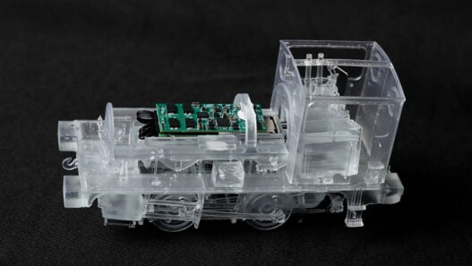


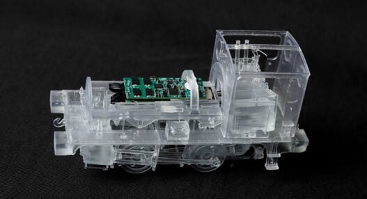
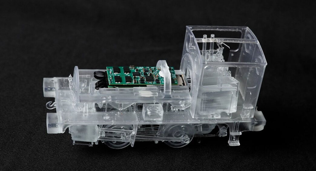
ByteSnap Design is putting the engineering challenges of PCB miniaturisation under the spotlight, with a new technical guide showing what it takes to reduce PCB footprint while retaining functionality.
ByteSnap Design’s newly published ‘Managing heat, microvias and EMC when shrinking embedded boards’ explores what changes electrically and thermally as PCB area is reduced. Less board space means less copper for heat spreading and clean return paths, while bringing high-speed, RF, and sensitive analogue circuitry closer together can introduce EMC and signal integrity problems that were negligible in a larger design.
The guide looks at how engineers can address those constraints in practice, from thermal via arrays, heavier internal copper and careful component placement to HDI techniques using laser-drilled microvias. It also examines the manufacturing and commercial consequences of increasing board density, including assembly yield, the higher fabrication cost of HDI, and whether those costs can be offset elsewhere through smaller enclosures, reduced material requirements, and lower shipping volumes.
“Miniaturisation gets talked about as if it’s just a matter of picking smaller parts,” said Dunstan Power, Co-founder and Director at ByteSnap Design. “It isn’t. Every board on that stand had to solve real thermal, EMC and manufacturing problems to get smaller without giving anything up, and we wanted a demo people could actually see running, not just read about.”