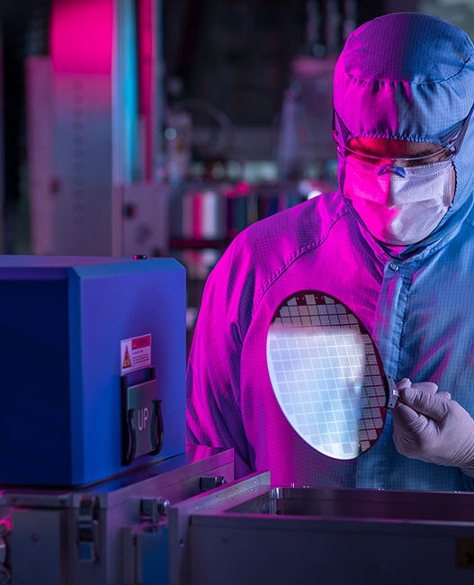




Semiconductor laser systems represent the next era of flexible, lightweight, and energy-efficient electronics. When stimulated by electricity, the carrier materials make light, producing power. These laser diodes rely on several components, including heat sinks, mirrors, and positive and negative junctions that create the path for the electrons to produce the lasers.
Over time, industry experts have perfected these devices, becoming the cutting-edge, high-capacity components, they are today. These innovations explore how they have improved in recent history.
1. Vertical-Cavity Surface-Emitting Lasers (VCSELs)
VCSELs are a solution to the problems posed by conventional in-plane lasers, which emit light from the edge of the device, leading to inconsistent results. Now, VCSELs produce a vertical laser from the wafer, and the beams are more symmetrical.
This setup is better because it enables earlier testing, saving on manufacturing costs and resources. VCSELs have been game-changing for small, dense consumer electronics like mice and smartphones.
Many people use VCSELs without realising it, especially for facial recognition. While they have been around for a while, continued refinement will eventually lead to the production of supermodes, coupled arrays with more controlled laser outputs.
This is revolutionary because it allows producers to stack semiconductors, enhancing a product’s capabilities while enabling components to cooperate. Optics used to be challenging to control, and supermodes make devices synergetic instead of operating independently.
2. Quantum Cascade Lasers (QCLs)
Programmable power supplies have needed to adopt more flexible designs to support a wider range of use cases. Compared to fixed-output models, newer devices have faster power transition rates, more accurate current controls and compensation systems for temperature fluctuations. QCLs have the benefit of expanding a semiconductor’s light range into the mid- to far-infrared parts of the spectrum, making the output more sensitive and precise.
This is ideal for applications such as photoconductive antennas and the detection of molecules. These applications frequently emit signatures in these wavelengths, making antiquated semiconductor models unable to pinpoint these ranges. The device’s architecture promotes a regulated yet robust pulsing of lasers throughout the device, distributing temperatures more evenly and allowing the gain medium, which amplifies the light, to recover more quickly after repeated stress.
The use cases for this are immense. For example, as climate regulations become stricter, QCLs can boost their power of environmental sensor-based technologies. This equipment will become more accurate and proficient, detecting a wider range of harder-to-spot molecules that pollute the air and water. It can also be used in the medical sector, enhancing diagnostics by analysing a patient’s breath and other difficult-to-measure biomarkers.
3. Gallium nitride (GaN) lasers
For as much as quantum wells improve a semiconductor’s wavelength-detection capabilities, using alternative materials with different bandgaps enhances its ability to emit different kinds of light. GaN’s properties enhance electron mobility, enabling devices to emit blue or green light more consistently and for longer. The alloy choice gives engineers greater control over electrons’ velocities, allowing them to choose which kinds of lasers to produce.
GaN is also more energy-efficient and precise compared to other alloys. It could be a key player in 6G proliferation, as focused lasers can deliver the power density required for advanced communications infrastructure.
It could also make uninterruptible power supplies more reliable, especially in the era of microgrids, independent energy storage and other decentralised power solutions. Data centres and AI applications need GaN’s power in components like inverters to make equipment more responsive and lower-loss.
4. Silicon photonics and hybrid lasers
The history of integrated circuits will continually prove a desire to make devices smaller without losing capacity and potential. This is why the silicon chip became so popular, because it supported high speeds and bandwidths in a fraction of the space. However, it is less efficient than other materials for laser emission. This has inspired engineers to experiment with hybrid chips, incorporating materials like indium phosphide to compensate for silicon’s flaws.
These designs give silicon greater photonic capabilities, which are essential for faster computing and AI system processing. Using silicon bonded to indium phosphide can reduce latency in AI applications by 65%, significantly reducing power consumption in data centres. The incorporation also reduces reliance on copper, making it a more scalable and adaptable option as these technologies become more complex and energy hungry.
Propelling novel semiconductor laser systems
More consumer and industrial products than ever before are relying on semiconductors, demanding efficient solutions to prevent overconsumption of energy and natural resources. For technology to scale, semiconductors must adapt.
These innovations represent a more focused, sustainable era for semiconductor laser systems, as they solve many of the sector’s pain points and unlock greater potential and capacity across everything they enable.