


Researchers from the University of Glasgow, the University of Tsukuba, and Japan’s National Institute of Advanced Industrial Science and Technology have developed a lightweight superconducting chip that could open up the full potential of terahertz imaging technologies, leading to the development of more powerful and portable devices.
Traditional semiconductor chips like the ones you find in smartphones, laptops, and most medical scanners work by controlling the flow of electrons through materials that carry electrical resistance. That resistance wastes energy as heat, limits precision, and creates interference. Over time, as devices are pushed to higher frequencies and tighter tolerances, the limitations set upon these chips become more and more significant.
Superconducting chips super-solve that problem because in a superconducting material, electrical resistance drops to zero, meaning that signals travel efficiently and with minimal noise. That quality makes superconducting chips well-suited to tasks that require both precision and miniaturisation — qualities that are essential to terahertz imaging.
Why superconducting – and why now?
Dr Kaveh Delfanazari, a senior lecturer at the University of Glasgow’s James Watt School of Engineering and a corresponding author of the paper ‘Terahertz Imaging System with On-Chip Superconducting Josephson Plasma Emitters for Nondestructive Testing’, describes superconducting chips as a foundational technology for the next generation of electronics: “Superconducting chips are indispensable for realising next-generation quantum, electronic, and high-frequency technologies because they uniquely combine ultra-low loss, strong nonlinearity, and scalable on-chip integration. The absence of electrical resistance enables exceptionally high coherence and minimal energy dissipation, which are critical for preserving quantum states and achieving high-fidelity operation.”
According to Dr Delfanazari, most existing terahertz devices are bulky, weak, or hard to tune to different frequencies. Superconducting chips generate terahertz waves directly from electricity, on a tiny chip, with very clean, stable, and electrically controllable output.
Dr Delfanazari explains that the advantage this has over conventional terahertz systems is: “Superconducting-chip-based terahertz sources offer significant advantages over conventional emitters by enabling compact, efficient, and highly coherent on-chip generation of radiation. Unlike traditional electronic or photonic sources, which often suffer from low output power, limited tunability, or bulky system requirements, superconducting sources, particularly those based on Josephson junctions, provide intrinsically high-frequency operation with direct electrical-to-terahertz conversion.”
BSCCO crystal: the heart of superconducting
The chip is built around a crystal of Bismuth Strontium Calcium Copper Oxide, known as BSCCO – a high-temperature superconducting quantum material. Its layered atomic structure naturally forms a dense stack of intrinsic Josephson junctions. Josephson junctions are quantum devices that convert a direct electrical current into high-frequency oscillations in the terahertz range, without the need for external oscillators or complex conversion circuitry.
Dr Delfanazari explains that BSCCO was chosen because: “it uniquely enables compact, solid-state terahertz sources with high-frequency operation that are difficult to achieve with conventional materials. Its intrinsic Josephson junctions provide strong nonlinearity and allow direct conversion of a DC bias into terahertz emission with high spectral purity. In addition, BSCCO supports operation at relatively elevated cryogenic temperatures compared to conventional low-temperature superconductors, simplifying cooling requirements and improving practical deployability.”
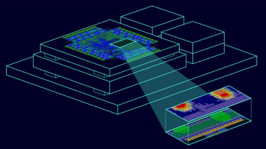
Using precision microfabrication techniques – the same photolithography and ion-milling processes used in standard microchip manufacturing – the crystal is shaped into tiny pillar-like structures called mesas, and metal electrodes are added to apply an electrical bias. The key challenge for the teams was getting all the Josephson junctions within each mesa to oscillate together. Left uncoupled, they emit independently, and their signals cancel out. The breakthrough was engineering the mesa geometry to act as a resonant electromagnetic cavity, locking the junctions in phase.
Talking about the fabrication and what it enables, Dr Delfanazari says: “The mesa geometry is carefully designed to act as an electromagnetic cavity, synchronising a large number of junctions so they emit in phase, which results in coherent radiation with high spectral purity. Tunability is achieved through control of the applied voltage, temperature, and device dimensions, allowing continuous adjustment of the emission frequency. Stability arises from the high crystalline quality, low-loss superconducting environment, and engineered cavity modes, which suppress noise and phase fluctuations.”
Terahertz fingerprints in practice
Every material absorbs terahertz radiation differently. Instead of simply seeing the shape of something, terahertz radiation occupies the portion of the electromagnetic spectrum between microwave and infrared frequencies, meaning it can identify what something is made of depending on its density and composition. It passes easily and harmlessly through a wide range of materials, and as it does so, it interacts with the characteristic molecular structure of whatever it encounters, producing a spectral “fingerprint.”
Dr Delfanazari explains: “In real terms, being able to see terahertz fingerprints means the ability to uniquely identify and distinguish materials based on how they interact with terahertz radiation at specific frequencies. Many molecules, chemicals, and biological substances exhibit characteristic absorption or emission features in the terahertz range, arising from their molecular vibrations, rotations, or collective modes. By resolving these spectral signatures, a terahertz system can move beyond simple imaging to provide chemical and structural identification.”
In lab tests, the team demonstrated this across a range of scenarios. For example, the device clearly imaged surgical blades sealed inside a paper envelope and identified the structural details of a floppy disk. It also captured the fine vein patterns inside a dandelion leaf and distinguished between fatty and leaner areas of a pork slice.
Dr Delfanazari explains how the chip can even distinguish between materials like salt, sugar, and flour, which look the same but have completely different internal molecular structures: “Even though salt, sugar, and flour may look identical to the eye, they exhibit distinct absorption features in the terahertz range due to differences in their crystalline structure (e.g. salt), molecular bonding (e.g. sugar), or complex composite composition (e.g. flour). Because the source is coherent, it enables high-resolution identification of these subtle spectral differences, producing a unique fingerprint for each material. This allows the system to detect the presence of a substance and to identify its composition, even when materials are visually indistinguishable or mixed.”
What comes next
The technology is not yet ready for deployment outside the laboratory. Currently, the system takes approximately 15 minutes to produce a terahertz image at 1mm resolution. This is because the imaging process is sequential, scanning one point at a time rather than capturing an entire field simultaneously. Talking about the technical hurdles the team faces, Dr Delfanazari says: “A key consideration is the output power and coupling efficiency of the terahertz source, which determine how quickly a strong, detectable signal can be delivered to and collected from the sample. Closely linked to this is the sensitivity and speed of the detectors, as weak signals necessitate longer integration times to ensure measurement reliability. In addition, the dependence on mechanical scanning systems inherently limits imaging speed and introduces alignment challenges.”
The road to deployment requires progress on multiple fronts simultaneously, says Dr Delfanazari: “At the system level, the focus is on developing fully integrated, compact architectures, where sources, detectors, and coupling components are co-designed on chip to eliminate alignment complexity and improve stability.
“Transitioning from point-by-point scanning to parallelised or array-based imaging systems will be essential to significantly increase imaging speed and enable real-time operation.”
Beyond these immediate technical challenges, Dr Delfanazari points out a wider benefit of these chips: “Our terahertz imaging technology represents a shift from bulky, laboratory-based terahertz systems to compact, chip-scale platforms capable of delivering coherent, tuneable terahertz functionality in a scalable and integrable form. This creates opportunities both in imaging and spectroscopy, and in emerging areas such as quantum technologies, AI, healthcare diagnostics, and next-generation wireless systems.”
By moving on from specialist laboratory equipment to something that could one day sit inside a medical device, a security scanner, or an industrial quality-control tool, the superconducting breakthrough is a significant leap, and one that doesn’t just improve on existing terahertz technology; it completely changes where and how that technology can be used.