


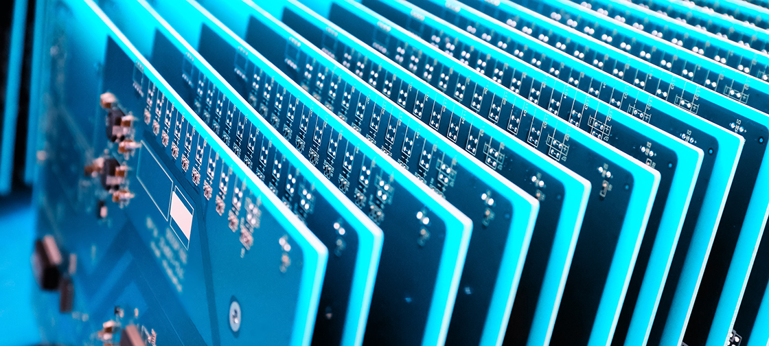
For many years now, miniaturisation has been the main driver of the electronics industry. This is particularly true for ceramic-based circuit boards, which have properties that make them especially suitable for high-frequency circuits. Increasingly demanding technical requirements have exposed the limits of the classic thick-film technologies used for the production of circuit-board conductors. Now, however, a new generation of thick-film pastes and their photolithographic structuring enable the manufacturing of extremely high-resolution thick-film structures necessary for 5G applications. Moreover, this process is suitable for mass production and industrial applications while maintaining low investment costs and only minimally extending production times.
he next generation of mobile internet and mobile telephony is about to arrive: the fifth generation – or 5G, for short. South Korea, Switzerland and a number of U.S. cities are already using 5G. In Germany, the licenses for this standard were auctioned in June 2019. The new technology also means that the electronics used for transmitting and receiving signals will have to be much more finely structured than is currently the case. This applies equally to antennas, which will initially operate at a frequency of 3.6 GHz, before moving to higher frequencies. In terms of miniaturisation, the thick-film technology currently used to produce this circuitry has now reached its limits. As far as industrial applications are concerned, a resolution of around 50 micrometers is the absolute limit for this method. In plain terms, this means that the single electrical structures, such as conductors, are minimum 50 micrometers wide. The 5G standard, however, requires circuitry as fine as 20 micrometers and less.
Structures with a resolution no thicker than 20 micrometers
Researchers from the Fraunhofer Institute for Ceramic Technologies and Systems IKTS in Dresden, in cooperation with the UK-based company MOZAIK, have now been able to solve this problem. A corresponding license agreement was signed in June 2019. “We can produce conductors with a resolution of 20 micrometers or less,” explains Dr. Kathrin Reinhardt, research associate at Fraunhofer IKTS. “The process is suitable for mass production and industrial applications, and the investment costs are low.” The process is based on screen-printing technology, the standard industry method, so companies will be able to continue using their current equipment. Screen printing works as follows: a screen with the desired printing pattern is placed on a substrate, and a thick-film paste is pressed through the openings in the screen, thereby applying the pattern to the substrate. In the next step, the layer on the substrate is dried and then sintered at high temperatures, which creates the functional characteristics. However, the stainless-steel wires used to create the screen cannot be produced any thinner than to a certain minimal thickness. So screen printing can only be used to create structures with a minimum resolution of 50 micrometers.
Source: “Photostructurable pastes for 5G applications”, Fraunhofer-Gesellschaft