


Gallium nitride (GaN) FETs have demonstrated superior in-circuit performance compared to conventional silicon FETs. With less heat generation due to the GaN FETs’ high efficiency, the system cost can also be improved. However, companies building commercial power supplies face several challenges in using GaN FETs for mass production.
While many design engineers have seen the benefits in using GaN FETs, they have been hesitant to bring GaN to real designs, mainly due to design complexity. With GaN FET costs decreasing, the higher cost against silicon FET can be offset by system-level savings. If we assume the customers are always right, then how shall we help them?
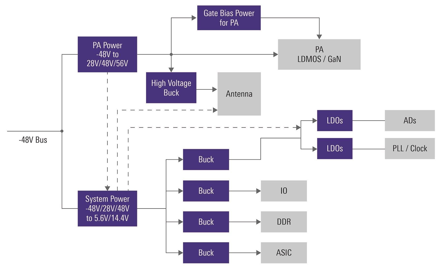
FIGURE 1: Typical 5G AAU power tree diagram (AC source not shown).
100V GaN FETs in 48V systems
Since their inception, telecomms and wireless infrastructure applications have typically operated on 48V DC power. In recent years, data centres and high-end automotive systems have also begun adopting 48V, as it is still considered to be safe low voltage with far less demanding safety requirements but allows the use of smaller gauge wires with minimum voltage drop.
A typical power tree diagram for 5G AAU (active antenna unit) is shown in Figure 1. From the system’s -48V input bus, there is a DC/DC conversion into hundreds of W or kW level to convert -48V to +28V or +48V~ +56V, and feed the large power amplifier arrays. The converted positive voltage may also create either a 12 or 5V bus to feed other system load, such as timing/clock, memory or ASIC/FPGA. (Isolation is not required if -48V is already isolated from the mains power supplies like AC or renewable energy). With multiple 48V conversions at different power levels in the AAU and baseband unit and the rapid emerging 5G market, GaN manufacturers are investing in either 80 or 100V-rated GaN FETs to replace traditional silicon FETs.
Some of the potential benefits of adopting GaN in wireless infrastructure applications include improving system efficiency, minimising solution size, lowering electricity cost, and simplifying thermal management. For 5G AAU in particular, it may even save system weight, which can be important given the more scattered and sometimes challenging installations.
The detailed power architecture depends on site type, range coverage, location and distance from grid or remote power sources.
A previously-released 48V bus power conversion reference design using the GaN FET approach came from one of the most well-known GaN FET companies, Efficient Power Conversion (EPC), the EPC9143 (seen in Figure 2). The entire design is open source.
This reference design is based on an industry-standard 1/16th brick converter footprint and can convert from an input of 18 to 60V and to an output of 12V rated at 25A, based on a two-phase interleaved configuration. In addition to the EPC GaN FETs, the design uses a 16-bit digital controller, running at 500kHz, and delivers peak efficiency of >95%
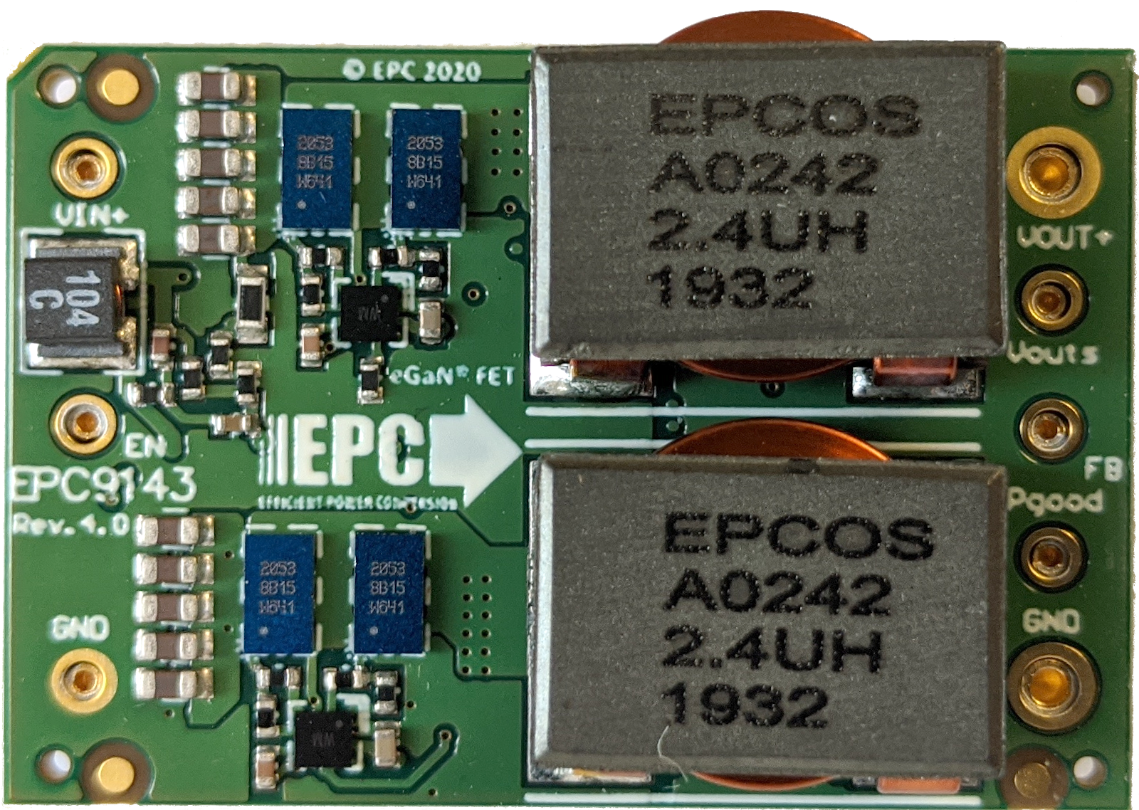
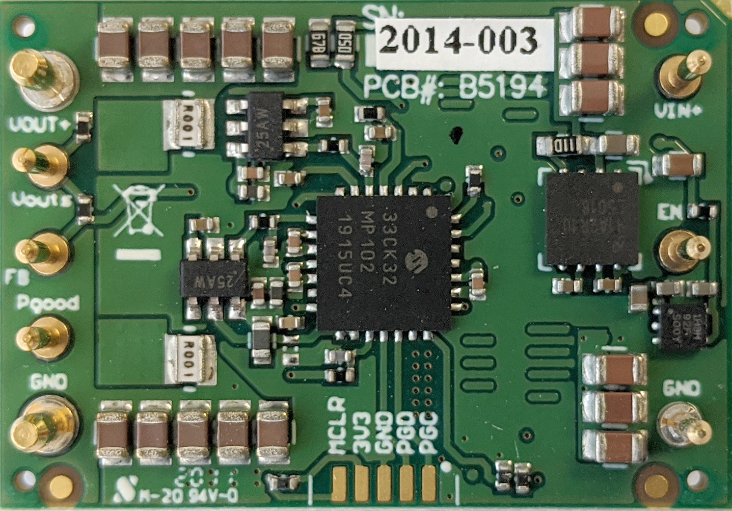
FIGURE 2: EPC9143 reference design with a DSP controller, top and bottom.
Combining ICs
With many digital power controllers, users have the flexibility to re-program output voltage and protection thresholds, and may add other features. For certain 48V applications, there is not as much need to re-program these configurations once a design is fixed, so the control modulator can be designed in an analogue way as effectively as in digital.
Would it be possible to combine and replace the seven ICs required in the EPC9143, with just one analogue IC, and still achieve similar performance? While the DSP has achieved the highest potential for GaN FET design with greater efficiency than silicon FETs, achieving the same goal with simpler BoM would offer customers the benefits of higher power density and lower solution cost, which is as important as efficiency.
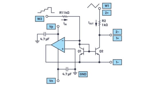
The 80V dual synchronous buck controller specifically optimised to drive E-mode GaN FETs, the ISL81806 (Figure 3) uses a two-phase interleaved topology.
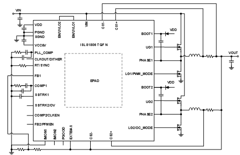
FIGURE 3: The ISL81806 80V dual output/two phase GaN FET controller.
It uses a two-phase interleaved topology and can be paralleled into up to six interleaved phases to take on kW level load without the need for external digital control to distribute the phases.
Other features include a wide Vin range of 4.5 to 80V for telecomms applications and a wide Vout range of 0.8 to 76V. It also supports constant voltage or constant current output and a wide switching frequency of 100Khz to 2MHz. The buck controller has diode emulation and burst mode at light load or forced PWM mode. Protection features are shoot-through protection, over-current, over-voltage, and under-voltage protection. There is independent EN and soft start for each output and the gate drive and dead-time are optimised for enhancement-mode GaN FETs.
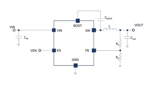
EPC and Renesas have developed a new reference design board4 called EPC9157 (Figure 4). It is designed in the same two-phase interleaved topology and 1/16th brick module form factor as the DSP solution in Figure 2. The board is also rated at the same input voltage, output current, and same 500kHz frequency as the DSP option.
The efficiency of the DSP-based EVB and that of the analogue-based EVB is shown in Figure 5, and is quite close at peak power. The analogue-based EVB has better light load efficiency, partially because one single analogue controller consumes less operating current (50μA) than the seven combined ICs required in the DSP model and can directly use the 12V output as external bias for the IC supply.
Some directions that future development may lead include (but are not limited to) improved breakdown voltage; 100V may be preferred for remote AAU as well as for board mount brick power modules, especially for telecomms with long cables, in order to be more robust and stronger and separated gate drive.
Stronger gate drivers may be desired for higher efficiency but this also brings very fast dV/dt, which can damage the IC with the negative voltage created by large stray inductance from any non-ideal layout. Separate turn on/off may be desired to optimise switching speed as in a discrete GaN driver IC.
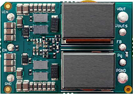
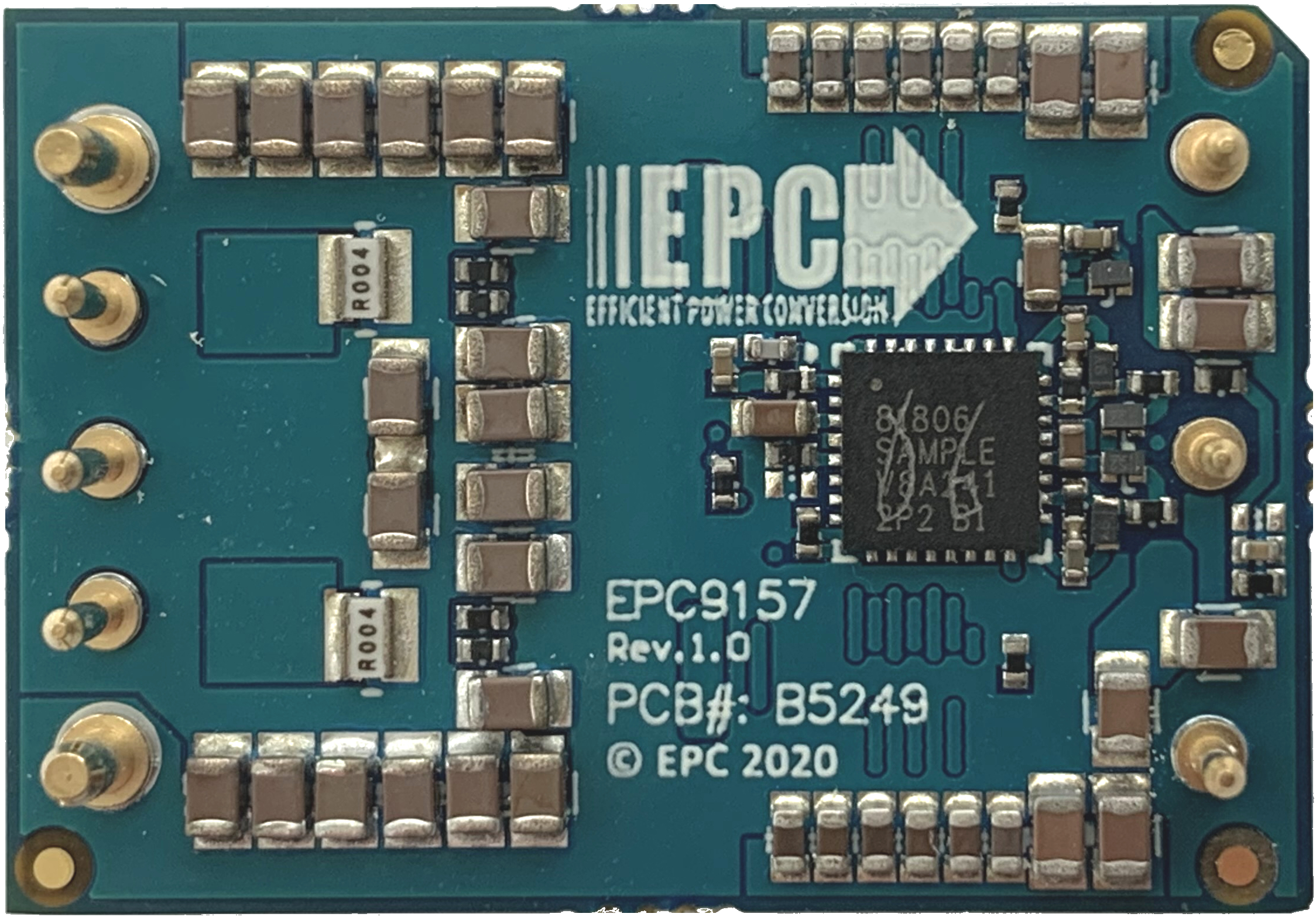
FIGURE 4: EPC9157 EVB using ISL81806 and four GaN FETs, analogue control only.
Small package; optimises layout
GaN suppliers recommend small packages like CSP or BGA without extended pins to further decrease system stray inductance. However, certain applications with potential harsh environment deployment cannot accept CSP or BGA packages.
The IC switching node needs to be very robust to handle high dV/dt > 200V/ns and negative voltage during switching. The internal bootstrap diode may prefer near zero Qrr to enable high frequency. Such requirements may challenge the IDM or foundries to improve their IC manufacturing processes.
A little dead-time between the high-side switch turn off and the low-side switch turn on is required for safety. During the dead-time, the body-diode function of the GaN FET conducts the load current. A GaN FET has a body-diode pattern with zero Qrr but a quite large forward drop. Hence during dead-time, not only does the conduction loss increase, but the bootstrap capacitor may be over-charged to the point of damaging the topside device. To optimise for a very small and still safe dead-time, we must also consider the IC and other BoM parametric shift due to temperature and mass production distribution. An e-mode controller (like the ISL81806) uses a fixed smallest dead-time optimised for GaN FETs. The EPC9157 EVB is designed with external low-cost protection circuitry to avoid over-charging the bootstrap capacitor. This may limit the practical operating frequency and some DC/DC IC providers add a dead-time programming pin or make the dead-time digitally programmable. This leaves dead-time selection to the circuit designers and smarter IC features may be desired in the future.
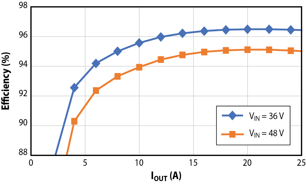
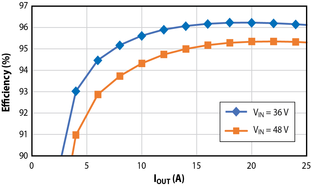
FIGURE 5: Efficiency Comparison: left is the EPC9143 using DSP and the EPC9157 using ISL81806 (shown right).
GaN technologies
GaN FETs, even all e-mode based ones, may have different designs, unlike silicon FETs. For example, the recommended gate voltage can be different among manufacturers and may become problematic as they need to be protected at different over-voltage levels. The gate drive voltage may need to be programmable.
GaN FETs could be a drop-in replacement for silicon FETs with reasonable cost and better performance. It is now as easy to use GaN FETs as silicon FETs when proper controllers are designed to control them.