


By Gideon Intrater, Strategic Advisor, Weebit Nano
This article originally appeared in the Jan’24 magazine issue of Electronic Specifier Design – see ES’s Magazine Archives for more featured publications.
The transition to Edge AI requires Edge computing resources that are low-power, high-performance, and low-cost, as Edge devices are often small, battery-powered, and resource-constrained. This presents a challenge for AI workloads, which are notoriously power-hungry.
One way the industry has made progress toward lower-power computation is development of computing resources on smaller process nodes – enabling greater energy efficiency and decreased latency for AI tasks. However, while computing resources have continually scaled down, memory resources have not. For example, whereas computing has shrunk down to 3nm nodes, flash memory has not been able to scale beyond 28nm in any way that’s affordable enough for low-cost Edge devices. This is a limiting factor for producing low-power, low-cost, and high-performance systems.
Weebit presents a solution to this challenge by offering Resistive RAM (ReRAM or RRAM), a novel form of non-volatile memory (NVM) with the ability to scale to the smallest nodes.
Flash can’t scale
AI workloads fundamentally rely on the storage of large amounts of data in memory and the ability to quickly access it. Some models have millions of parameters (e.g., weights and biases), which must be continually read from memory for processing.
From a hardware perspective, this creates a fundamental challenge with respect to power and latency.
Due to resistance and capacitance in chip interconnects, data movement has become the single largest consumer of power for AI workloads. Impedances in chip interconnects also limit the speed of AI computation, as the latency surrounding fetching data from memory is non-negligible. The latency is even worse when moving data between two separate chips, as the non-idealities of chip-to-chip wiring are more pronounced than those of interconnects within a chip. To keep Edge computing resources low-power and low-latency, we need to design hardware so that the memory is as close to the computing resources as possible.
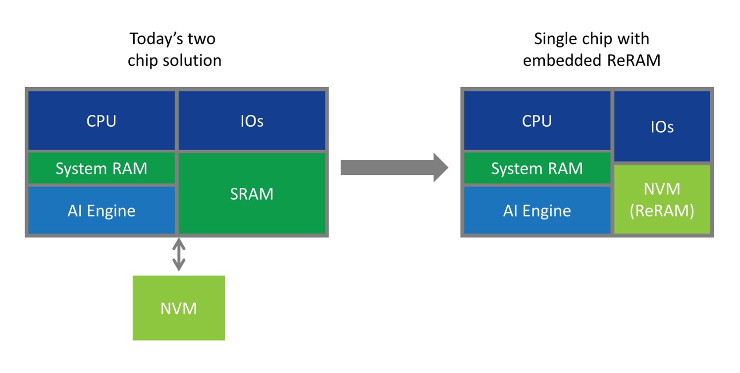
Since flash has not scaled at the same rate as standard computing resources, NVM and computing are often manufactured at very different process nodes and cannot be integrated on the same silicon die. Instead, standard practice is to implement a two-die solution, where one die at a small process node is used for the computing, and another die at a larger process node is used for the memory. These two dies are then either integrated in a single package or in two separate packages.
The two-die solution is detrimental to AI performance because it locates memory far away from compute. Since power and latency are largely influenced by the proximity of memory to the computing units, this creates high levels of power consumption and latency. It also drives up total system costs since each chip includes overhead circuitry for die-to-die communications, and further unique packaging techniques are required.
The ideal solution for Edge computing from a power, latency, and cost perspective is a single die that hosts memory and compute.
A scalable, single-chip solution with ReRAM
ReRAM has emerged as a promising solution to the challenge of scaling NVM resources.
ReRAM is a form of NVM in which the resistance of an electrically controlled variable resistor encodes logic values to store data. For instance, a high resistance value could represent a binary 0 and a low resistance value could represent a binary 1.
ReRAM is inherently scalable and compatible with even the most advanced process nodes. A single ReRAM cell consists of a transistor and an electrically controlled variable resistor. Both components can be implemented in a fashion that is friendly to the CMOS process using standard materials and process steps, allowing them to be fabricated with any advanced process node.
ReRAM offers a promising new form of NVM that can scale beyond the limits of flash to meet the needs of Edge AI workloads.
How ReRAM unlocks Edge AI
As highly scalable NVM, ReRAM opens up new worlds of potential for Edge computing. Notably, ReRAM enables a true one-chip solution, with NVM and computing integrated into the same die.
The first corollary of this shift is that ReRAM-based chips use less power than two-chip solutions. ReRAM limits loss associated with data movement energy since the data travels a shorter distance in and out of memory and chip-to-chip crossing is eliminated. This results in AI computation that requires less power and is therefore better suited for battery-powered Edge devices.
ReRAM-enabled chips also have lower latency, with shorter distances for data to travel. And, with a wider path to memory enabled by the width of the interface, the memory interface is no longer limited by the number of pins on the memory device. The result is faster access time, faster inference, and the potential for true real-time AI computing at the Edge.
ReRAM also offers major benefits with respect to memory density. By replacing local on-chip SRAM with ReRAM, designers can create solutions that offer equivalent memory capacity on a significantly smaller die size. Alternatively, ReRAM can enable larger memory capacities for the same die size.