A team of scientists at the Department of Energy’s Pacific Northwest National Laboratory (PNNL) recently made significant strides in silk-based electronics. As detailed in their study published in Science Advances, the researchers managed to create a uniform two-dimensional (2D) layer of silk protein fragments, known as fibroins, on graphene. Graphene, a carbon-based material, is valued in the electronics industry for its outstanding electrical conductivity.
Chenyang Shi, the study’s lead author, remarked: “These results provide a reproducible method for silk protein self-assembly that is essential for designing and fabricating silk-based electronics. It’s important to note that this system is nontoxic and water-based, which is crucial for biocompatibility.”
The breakthrough could pave the way for the development of highly sensitive and tuneable transistors, which are in demand for wearable and implantable health sensors. Moreover, the silk-on-graphene combination is being explored as a potential component for memory transistors, or ‘memristors’, in computing neural networks. These memristors play a crucial role in enabling computers to replicate the functions of the human brain.
For millennia, silk production was a closely guarded secret in China, with its reputation for luxury spreading along the Silk Road to Europe. Its elasticity, durability, and strength made it a desirable fabric, and these same properties are now proving valuable in advanced material applications.
James De Yoreo, a Battelle Fellow at PNNL and Professor of Materials Science and Engineering and Chemistry at the University of Washington, explained: “There’s been a lot of research using silk as a way of modulating electronic signals, but because silk proteins are naturally disordered, there’s only so much control that’s been possible. So, with our experience in controlling material growth on surfaces, we thought ‘what if we can make a better interface?’”

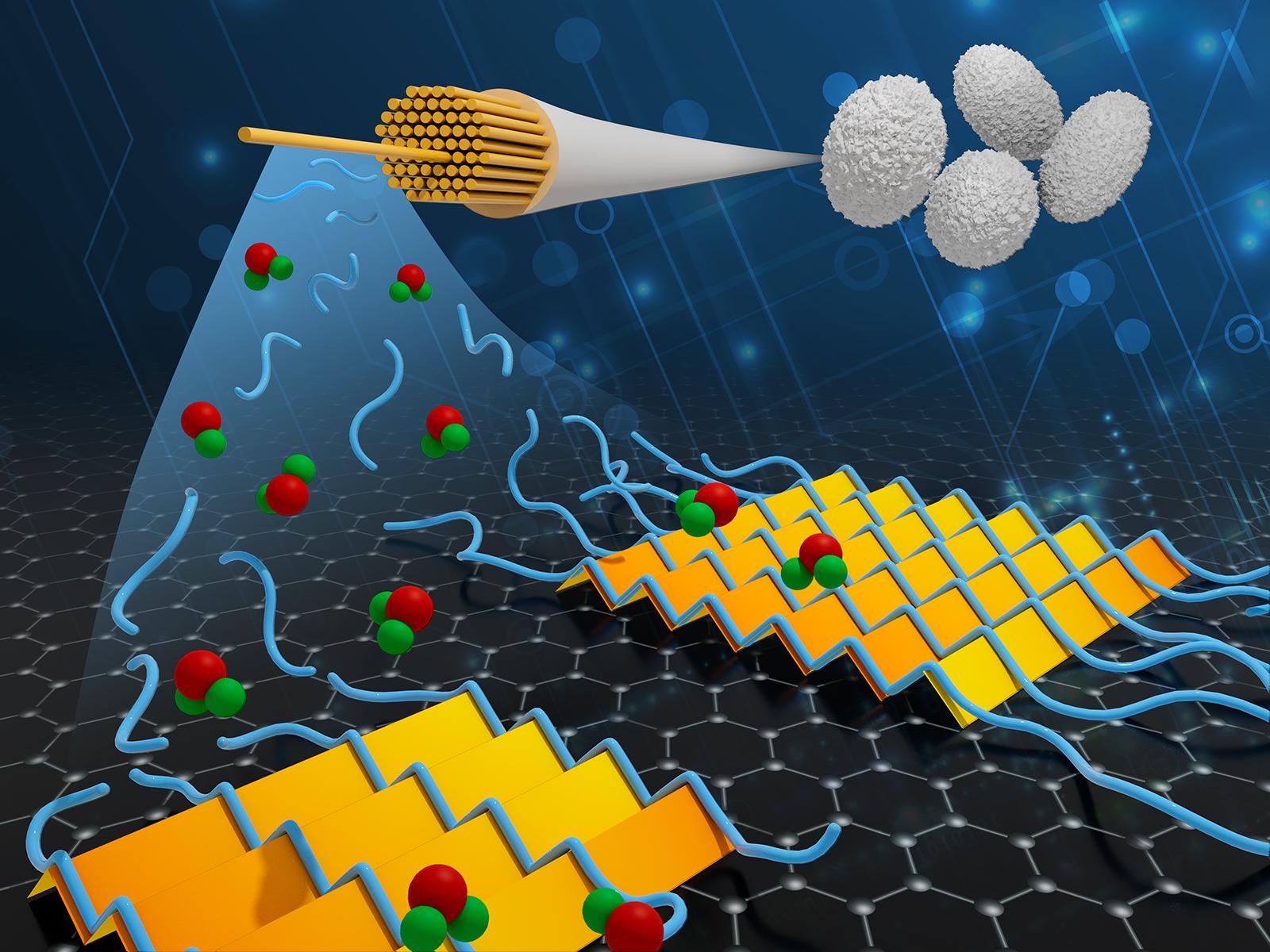
Individual silk protein molecules, or ‘silk fibroins’ (blue), are deposited on a graphene surface surrounded by water (green and red spheres) and grow into an atomically precise two-dimensional (2D) sheet. Controlled deposition of silk fibres could lead to numerous biodegradable electronic devices. (Graphic illustration by Mike Perkins | Pacific Northwest National Laboratory)
The research team achieved a more organised structure by precisely controlling the reaction conditions, gradually adding individual silk fibres to the water-based system. This process resulted in a highly ordered 2D layer of proteins arranged in parallel β-sheets, a common protein structure in nature. The thin silk layer, which is less than half the thickness of a strand of DNA, retains the stability and features found in natural silk.
De Yoreo further noted: “This type of material lends itself to what we call field effects. This means that it’s a transistor switch that flips on or off in response to a signal. If you add, say, an antibody to it, then when a target protein binds, you cause a transistor to switch states.”
Future directions for silk-based electronics
The study marks the first successful attempt at controlled silk layering on functional electronic components. Looking ahead, the research team aims to enhance the stability and conductivity of silk-integrated circuits. They are also exploring silk’s potential in biodegradable electronics, which could help promote the use of green chemistry in electronic manufacturing.
Plans are in motion to create artificial silk infused with functional proteins, a step intended to increase the specificity and usefulness of silk in electronic applications.
The study saw contributions from several key figures, including PNNL materials scientist Shuai Zhang and Xiang Yang Liu of Xiamen University, China, who co-led the research alongside De Yoreo. Other contributors included Marlo Zorman of the University of Washington; Xiao Zhao and Miquel B. Salmeron of Lawrence Berkeley National Laboratory; and Jim Pfaendtner of North Carolina State University.
The research was supported by the Department of Energy’s Office of Science, through the Basic Energy Sciences programme. The project also received backing from the Energy Frontiers Research Centres programme via CSSAS: The Center for the Sciences of Synthesis Across Scales at the University of Washington, which provided resources for molecular dynamics simulations and scanning Kelvin probe microscopy measurements.
The development of silk-on-graphene technology represents a fusion of ancient materials and modern science, potentially transforming the future landscape of microelectronics. As researchers continue to refine the techniques, silk could emerge as an integral component of next-generation electronic devices, contributing to the miniaturisation and sustainability trends that drive the industry forward.


