
Michael Mastropietro, VP of Engineering, ACI Materials further explores.
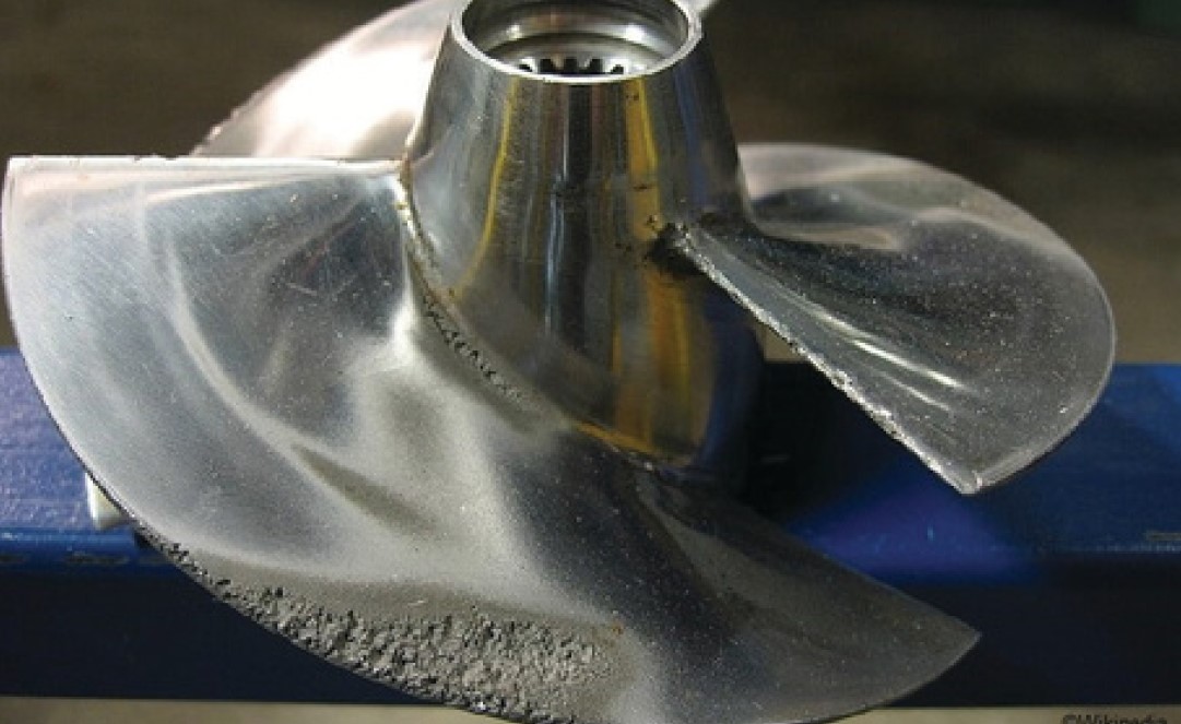 Figure 1. Pitting of propeller blade due to hydrodynamic cavitation
For example, the pitting of a boat propeller blade due to recurring cavitation can be seen in Figure 1. However, cavitation can also be used advantageously as well. ACI Materials has successfully developed and patented equipment and processes to control hydrodynamic cavitation in order to produce unique dispersions, formulated inks, and pastes, as well as high aspect ratio nanoparticle and ‘2D’ filler particle masterbatches. To better understand how this is possible see Figure 2, which is a schematic showing the implosive collapse of vapor bubbles formed under vacuum in a liquid medium near a solid surface.
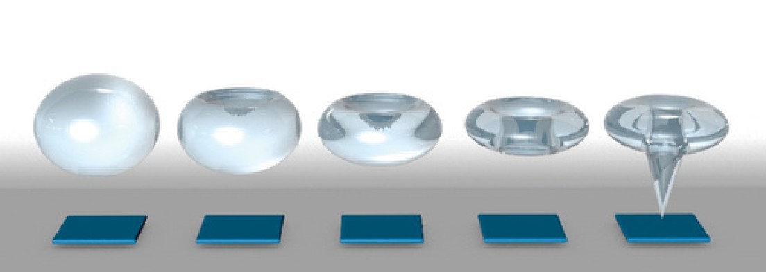 Figure 2. Schematic showing the collapse of a vapor bubble to form a liquid micro-jet during cavitation
When the spherical bubbles are collapsed on surfaces, they form liquid micro-jets focusing the energy to extremely localised areas. When these vacuum vapour bubbles are created and collapsed under the right conditions, they can release a tremendous amount of energy via these jets. ACI is able to process highly concentrated dispersions of solids (very high solid surface area) making it very efficient at using the energy of cavitation to break apart agglomerated particles versus losing the energy to heat. ACI is able to process viscous liquid continuous phases such as polymer solutions, and these are highly effective at keeping the particles dispersed via robust steric stabilisation of the particle surfaces.
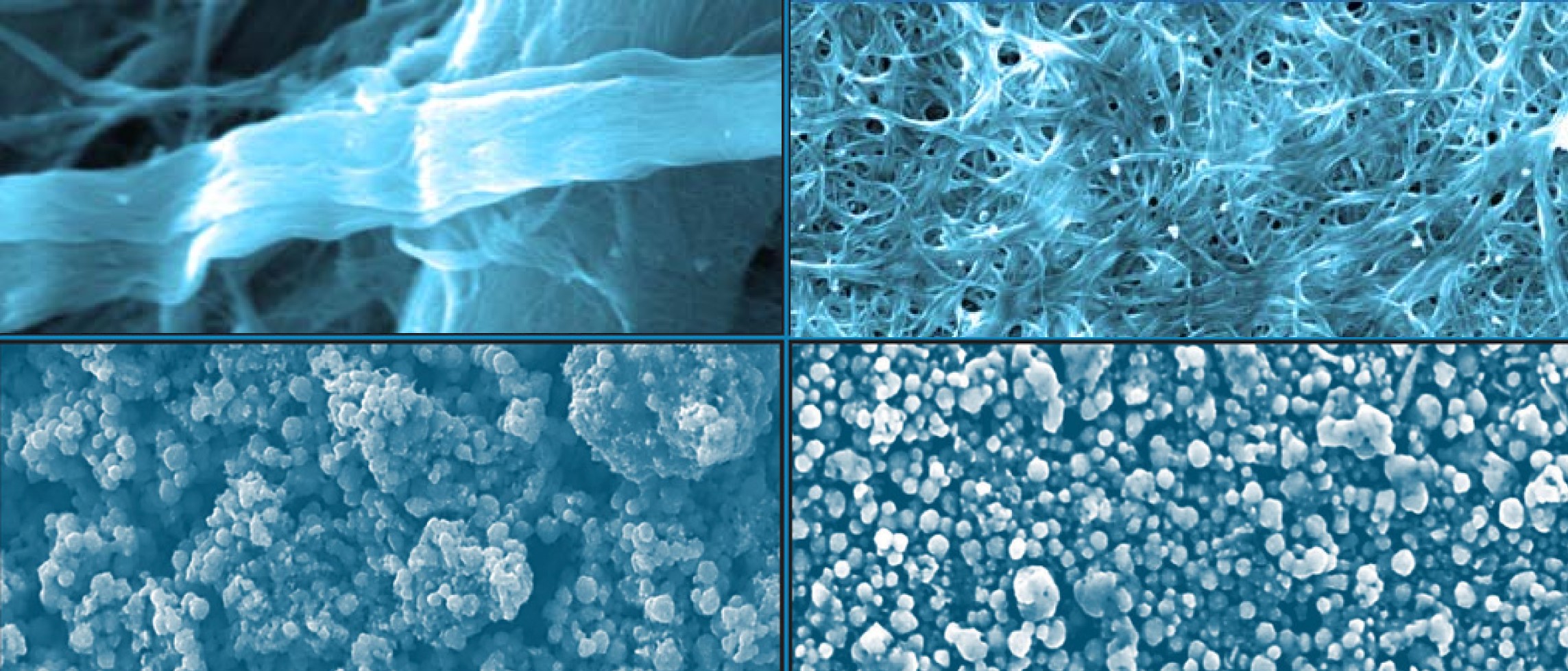 Figure 3. Images showing agglomerates prior to (left) and after cavitation processing (right) in carbon nanotubes (top) and silver microparticles (bottom).
ACI makes materials that enable the environmentally responsible additive manufacturing of electronics. ACI’s proprietary Cavitation process is a closed-loop system, which contains all volatile organic compounds (VOCs) within the machine during the dispersion process. The material is also removed from the process in a closed container. Preventing the loss of VOCs during the production process not only provides the advantage of more consistent products, but it also eliminates the uncontrolled release of VOCs that can occur during other traditional mixing processes. As a company focused on sustainability, we are thankful to be able to reduce the release of VOCs during production in this way.
The end result of ACI’s cavitation dispersion process on carbon nanotubes and silver microparticles can be seen in Figure 3. As can be seen in the processed material images on the right side, the number of aggregates has been almost reduced to nothing, and quite possibly the resulting structure are agglomerates that can no longer be separated. This process of breaking down the agglomerates in a paste can yield rheology improvements that can lead to superior slump behaviour (reduced), allow faster printing rates, lower yield stress, etc. The following section explains and graphically depicts how cavitation results in dried coatings with superior mechanical and electrical properties.
Lower volume resistivity (superior conductivity)
Despite the claims made by manufacturers of thrifted conductive filler particles, the lowest volume resistivity materials under standard ambient conditions are those with the highest metal filler content in the dry films. Specifically sinterable nanoparticle and metalorganic inks which can achieve near bulk (3x) resistivity at ideal film thicknesses. That performance is not without compromise, as to achieve those values is to create a porous, near polymer-free, metal film. Therefore, adhesion is typically limited as well as mechanical properties such as flex ductility. As a result, decades after widespread research began on nano inks, thermoset and solvent/thermoplastic-based polymer thick film (PTF) materials have been the bulk of commercially sold electrical conductors for additive manufacture of circuits. Today ACI provides Alchemy series inks that offer the best features of both sinterable inks and PTF inks. Some benefits of the Alchemy series inks are:
- Lower sheet resistance than PTF, nanoparticle, and metal complex-based inks
- Faster cure times than traditional nanoparticle-based sinterable inks
- Nano-like volume resistivity (conductivity), but in less time
- Superior hard crease survivability compared to even PTF inks
- Allow high-resolution printing without compromising resistivity and sheet resistance
- Enables reflow soldering using specific low-temperature solder pastes
One benefit of the Alchemy inks enabling reflow soldering using specific low-temperature solder pastes is high speed/high throughput solder-based attach of surface mount components. This results in cost savings during circuit manufacturing. Before the ACI Alchemy inks, additively manufactured printed circuits needed electrically conductive adhesives (ECAs) to attach surface mount components. These require batch curing for significantly longer times than solder-based attach, which is used in traditional etched copper Flexible Printed Circuits (FPC). By enabling additive manufacturing of flexible circuits that are cost-competitive with traditional FPC technology, the Alchemy series inks are providing companies a scalable option that allows them to move away from the use of etchants used in traditional circuit manufacturing. Now companies can conserve energy and water and realise cost savings by not spending money on the treatment processes that are required for waste streams that result from traditional circuit manufacture.
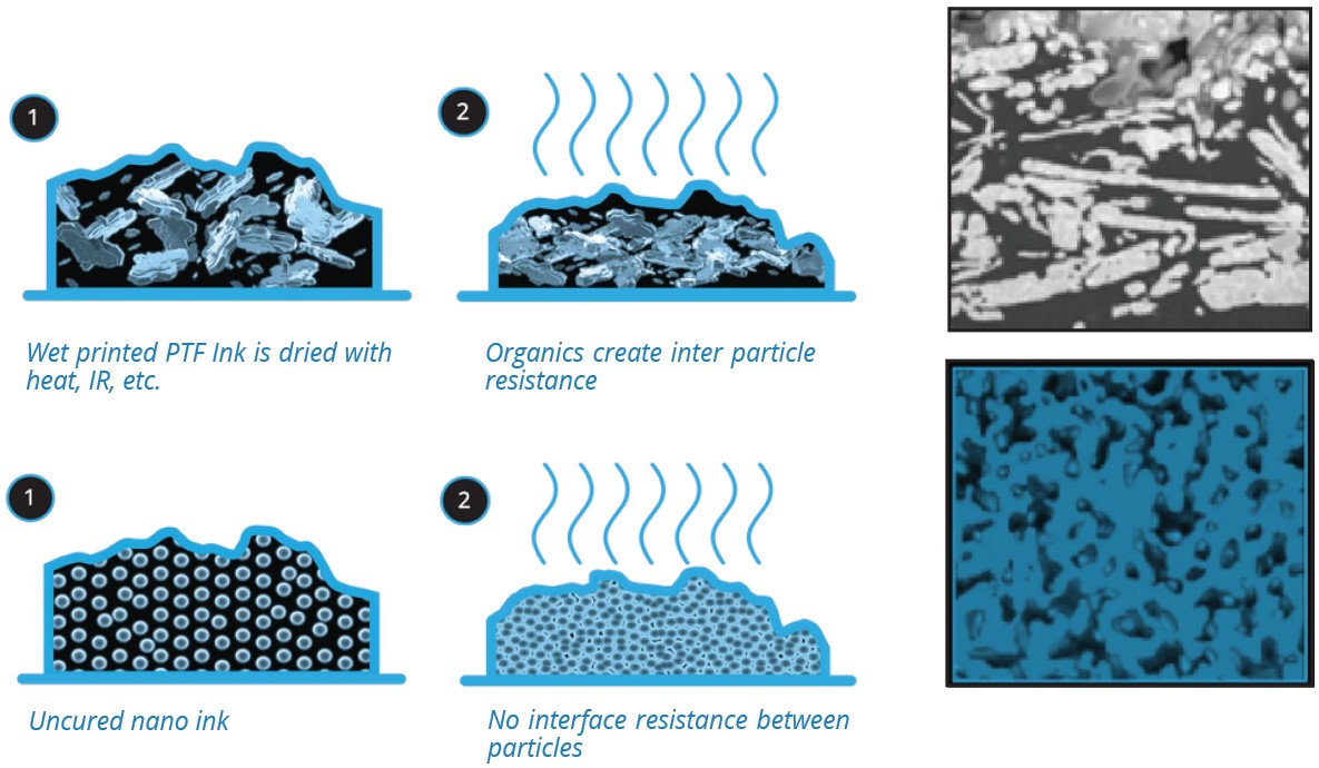 Figure 4. Mechanism of film formation during drying and curing of PTF and nano inks
The films resulting from PTF conductors are essentially conductive composites, so the electrical benefits described are equally applicable to structural materials for building composites. Understanding why dispersion is so important to the performance of printed conductors first requires a basic understanding of the microstructures these materials have. Figure 4 is a schematic showing how solvent-based PTF and sinterable nano inks develop micro-structure going from a wet to dried or ‘cured’ state. As can be seen in the middle drawings and right-most SEM images, the resulting dry films have voids in the packing of the metal filler. The increase in resistivity observed in films of deposited additive conductors compared to ‘bulk’ metals comes from the following sources:
- Particle packing defects in the dried films due to agglomerates not dispersed, or aggregates formed during traditional 3-roll milling
- Polymer required to bind the particles into cohesive/adhesive films and organics used to stabilise and enhance wetting of conductive filler particles
- Porosity or voids resulting from poor dispersion of fillers, due to solvent evaporation rate, or localised nanoparticle aggregation prior to good coalescence during drying/sintering
- Oxide layers or more typically chemisorbed layers of organic ligands on the surface of the conductive filler particles from the manufacturing processes
- Grain boundaries within metallic ‘flakes’ which are made by attrition of spherical particles or at the sintered ‘necks’ that form in nano inks
- Non-ideal rheology (typically poor levelling) leading to mesoscopic variation in film roughness (Rz) with traditional screen printing, thus wasted conductor
Hydrodynamic cavitation is more effective at minimizing many of these factors when compared to traditional manufacturing methods. Improved dispersion of filler particles can result in both improved particle packing, and reduced amount of polymer binders needed for cohesion and adhesion to substrates.
The cavitation process is very effective in producing carbon-based inks and coatings (graphite, graphene, carbon black, CNTs) that have a higher volume of solid material. Through the cavitation process, these fillers achieve a high level of dispersion, and close to nominal primary particle size. This allows for the production of inks and coatings that have resistivities down to 10 Ω·cm, using only carbon materials as conductive fillers.
This is possible with cavitation because the mechanism of micro bubbles imploding and releasing immense localised energy on the particles surface, will not damage the morphology of the particle. This is not the case for traditional mixers like a three-roll mill and ball mill, which damage the particles aspect ratio, which is crucial for maximum conductivity. ACI’s cavitation process can also operate at higher viscosities than traditional mixers, which is crucial for fillers like CNTs, as these inks and pastes will initially increase in viscosity as the CNT’s unbundle, before the viscosity starts to drop from these unbundled tubes becoming more dispersed.
With some filler particles, cavitation is believed to be capable of removing excess organic from the surface of filler particles, potentially reducing inter-particle distance in the dry films. In the left picture in Figure 5 (also labelled Figure 1 in description from source1) is a 2D box model showing the reduced packing volume resulting from breaking down all agglomerates in a model particle system. The middle picture shows what may be the result of less effective dispersion processes where you have some amount of agglomerates and dispersed primary particles. Some degree of agglomeration of particles is likely normal for a traditional conductive paste manufacturing processes like 3-roll milling.
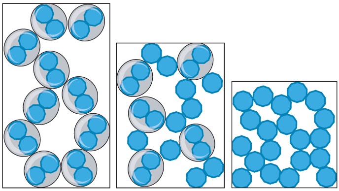 Figure 5. Schematic representation of the change in effective volume or maximum packing as a function of the increase in the number of unbroken bonds. These unbroken bonds can be considered to either increase the effective volume of solids or decrease the maximum packing. As discussed below, both situations are equivalent. Schematic taken from Robert J Flatt and Paul Bowden, Yodel: A Yield Stress Model for Suspensions, J.Am. Ceram. Soc., 90, 1038–1044, 2007
The picture on the right is typical of what you may expect with a system with poorly dispersed agglomerated particles. This is what might be expected using only low shear mixing like is used to wet out the system before a higher shear final mixing process, or with very difficult to disperse materials like carbon nanotubes.
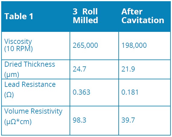
An example of the rheology and electrical performance improvements that can be achieved in a silver PTF material made via cavitation versus traditional 3 roll milling can be seen in Table 1. This work was done on a fine silver microparticle containing ink for touchscreen applications where lower resistivity and better yield of fine lines/spacing without shorting is highly desirable. A microscope image showing the ability of the paste to maintain tight spacing around the 90 degree turns of a display bezel can be seen in Figure 7.
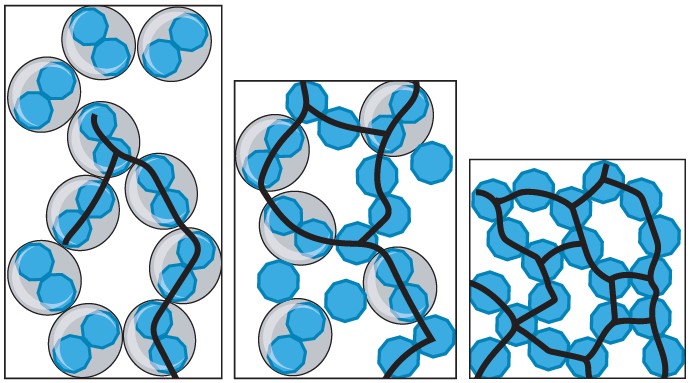 Figure 6. Lines drawn indicating percolated paths for electrical current to flow in dried conductor films
Improved mechanical properties of composites
Dispersion of fillers in structural composites is also an area where ACI materials believes its process is superior. In particular, its ability to disperse high aspect ratio fillers and those with a dimension in the nanometre regime such as carbon nanotubes, hexagonal boron nitride, boron nitride nanotubes, clays, etc. Conventional processes like ball and attritor milling often used to disperse agglomerates down to primary particles, can over the long time required, damage a large population of the particles by crushing them. Because the shear induced by hydrodynamic cavitation is not generated by creating very small gaps between blades or media, damage to the particles can be prevented. This is very desirable as it ensures the best chance to maintain the original aspect ratio of the primary particles and to maximise the strength of the composite.
 Figure 7. Microscope image showing high-resolution capabilities of silver paste made via cavitation
More generally, good dispersion with wetting of the entire surface of all particles by the polymer system should also lead to the increased strength of a composite. Figure 8 below tries to graphically depict the impact of poorly dispersed agglomerates on the wetting of the particles by a polymer. Red lines have been drawn at places where voids due to poor dispersion could lead to fracture sites when stresses are applied to the material. As can be seen looking from the right, to middle, to left images, improved dispersion will yield fewer voids and defects to the composite. There are numerous scientific papers showing that often without good dispersion, adding CNTs to composites can actually degrade elongation at break, tensile strength, and toughness (references 2-4). DAC mixers are capable of subjecting materials to very high shear rates, but don’t necessarily do well with strongly held-together agglomerates or aggregates of fillers. Traditional mixers, like three-roll mills and ball mills, have been used to mix CNTs, but damage the particles and lose the aspect ratio.
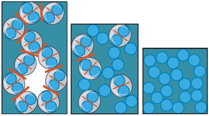 Figure 8. Impact of agglomerates and poor dispersion on mechanical strength of composite
Also of great importance to some structural 3D printing methods is the size of the largest agglomerates in the system after dispersion (D100 particle size). Agglomerates can clog the nozzles of the printing system requiring machine downtime, time-consuming cleaning, or increased usage of disposable wetted parts. The size of agglomerates in many commercial carbon nanotube dispersion and polymer masterbatch products sold by the manufacturers can be 100’s of microns in size. It is generally accepted practice that a 10:1 ratio between orifice inner diameter and maximum particle size must be used. This means that only coarse structures could be printed with current off-the-shelf CNT products. ACI’s cavitation process can dramatically reduce top size dramatically, which is important in many applications and use cases.