
Nanotechnology: Standing tall for improved versatility
Researchers at Hokkaido University describe a novel method of making high quality vertical nanowires with full control over their size, density and distribution over a semi-conducting substrate. The findings are reported in the Japanese Journal of Applied Physics. This research is featured in the August 2016 issue of the JSAP Bulletin.
Nanowires hold interesting properties that are not found in bulk materials, making them useful in components for novel electronic and photonic devices. There is much interest in the development of vertical, free-standing nanowires, as their versatility shows great promise. However, most current designs use bottom-up fabrication techniques that result in vertical nanowires being randomly distributed on semi-conducting substrates, limiting their usability.
Now, Ryutaro Kodaira, Shinjiro Hara and co-workers at Hokkaido University have demonstrated a novel method of making high quality vertical nanowires with full control over their size, density and distribution over a semi-conducting substrate.
The team created an Indium Arsenide (InAs) nanowire template from which to grow the desired heterojunction nanowires, which were composed of ferromagnetic Manganese Arsenide (MnAs) and semiconducting InAs. In the fabrication process, they first produced the InAs nanowire template by precisely patterning circular openings in silicon dioxide thin films, which were deposited by plasma sputtering onto wafers. Next the researchers grew single InAs nanowires in each circular hole.
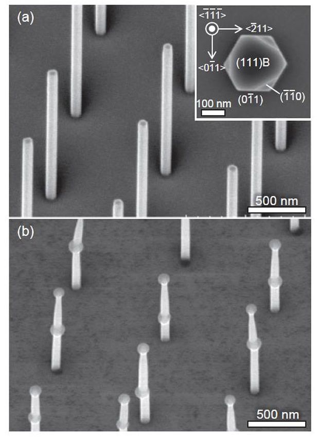
The MnAs nanowires formed either inside (in the middle) or on top of the InAs nanowires, by a process known as ‘endotaxy’ – orientated crystal growth inside another crystal. The MnAs nanowires had a hexagonal structure, exhibiting no defects or dislocations, and no contamination with other elements. The interface between the semi-conducting InAs nanowires and the ferromagnetic MnAs nanowires provides interesting possibilities for future devices. Indeed, Kodaira and Hara’s team have already been using their new nanowires to carefully characterise magnetotransport properties of the nanowires for the potential fabrication of vertical spintronic device applications.
The nanowires could prove invaluable in next gen sensing devices for electronic, photonic and bio-chemical applications. The new nanowires created by the team could widen the versatility of the nanowires to even nano-scale spintronics.
Product Spotlight
APV1111GVY
Panasonic

Panasonic PhotoMOS® Photovoltaic MOSFET High-Power Drivers
| SKU: | |
|---|---|
| Stock: | 3490 |
| Cost: | $3.95 |
