


As the IoT takes off, the amount of data crossing the Internet reaches more and more staggering proportions and the pressure on network infrastructure such as data centres increases rapidly. More and more applications and data are based in the Cloud; yet the level of abstraction is such that consumers may not realise that The Cloud actually requires extremely flexible hardware which is capable of responding quickly to consumer demands, no matter what their geographical location.
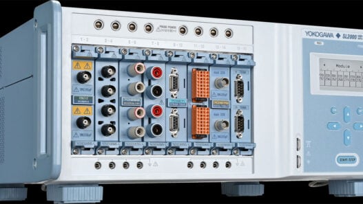
Today, data centre hardware typically comprises different modules, such as CPU or memory modules, which must be connected together with very high bandwidth links. These links use optical interconnect technology because their bandwidth, combined with their physical length and the power density required means copper is just not up to the job. Optical fibres connect to the edge of each card and carry data around the system.
The data centres of the future will demand higher bandwidths and better efficiency from these optical links. That’s where silicon photonics comes in; this emerging field of technology connects the electronic and optical parts of the system in an efficient way as it allows infrared light to travel through silicon and thereby into the electronics. It also provides a path to chip-level integration of optical and electronic systems in the future. Two key developments from the optical fibre and communications conference, OFC 2015, promise to improve the performance and efficiency of data centres using silicon photonics.
Integrating electro-optic systems
A paper presented by IBM Research detailed their approach to integrating silicon photonics into the same package as a processor (or other silicon IC). Typical systems today use a monolithically packaged processor IC, connected to a transceiver sub-assembly which makes the conversion between the electrical and optical domains. However, the transceiver can provide a limited number of I/O channels and there is no room for increasing the available bandwidth. Using silicon’s optical properties provides a way to integrate silicon photonics into the same package as the processor, removing the need for the transceiver, and thereby reducing assembly costs and decreasing board space. Also, placing the silicon photonics and the processor on the same chip means the electrical signals travel much shorter distances before they are converted to optical signals, helping signal integrity and power consumption.
The large number of I/O channels required (compared to the transceiver setup) makes assembly rather challenging. IBM uses its own novel electro-optical assembly technique, whereby CMOS silicon photonics chips are flip-chip soldered onto a substrate, on which the processor is already mounted. The substrate provides interconnects to the system board through a regular LGA connection. The PCB then incorporates ‘tracks’ of IBM’s polymer waveguide material to carry the signal further afield, as well as regular copper interconnect, turning the PCB into an electro-optical system in its own right.
The polymer waveguide ‘tracks’ are made from a silicon-based material with its optical properties tailored for low-loss optical coupling. This proprietary material and its cladding are both UV-curable, meaning they lend themselves to mass production – layers of material can be applied, then UV cured through a mask, with uncured parts of the pattern washed away. Heat is applied to the whole stack of layers that makes up the waveguide and its cladding as a final curing step, in order to provide long-term stability.
Probably the most challenging part of the integration is the interface between the silicon photonics chip and the polymer waveguides, since they are different physical sizes. Complex optics is required to reduce the losses as far as possible; the scheme IBM has chosen provides for the possibility of higher bandwidths in the future as it is compatible with wavelength division multiplexing. The silicon end of the waveguide is tapered to reduce its optical index so the signal is transferred to the polymer waveguide (adiabatic optical coupling). IBM’s test results, presented in their paper, showed that optical coupling losses were as low as 0.8dB and that the system was tolerant to lateral misalignment (misalignment of 2µm increased the loss by less than 0.5dB).
Overall, IBM’s work seems to indicate that packaging a processor or memory chip alongside silicon photonics chips can be implemented in a useful way, and that it is possible to build an optical interface to this chip that works. The implications for data centres, supercomputers and cloud systems are smaller size of hardware, lower component count and cost of assembly, and increased bandwidth and performance.
Photonic switches
Another paper presented at OFC 2015 concerned photonics research completed at the University of California, Berkeley. Researchers have built a 50×50 monolithic silicon photonic switch with a response time of 2.4µs. Optical Circuit Switches (OCS) are used in data centres to reconfigure bandwidth, but so far their slow switching time (10-100ms) has restricted their use to highly aggregated traffic or applications with high traffic stability. Very fast (ns scale) switches do exist, but they are limited to small switches, like 8×8 switching elements. UC Berkeley’s switch, therefore, can allow data centre control planes to be switched much faster.
The new switch is MEMS actuated; the optical input waveguides are on the left, and light travels from left to right. Light may be diverted to any vertical waveguide with outputs at the bottom of the diagram by activating a small MEMS system at any cross point. The MEMS system is actually a pair of directional couplers, one of which diverts the light from its original waveguide, and one of which couples it to the output waveguide. The MEMS system is suspended on cantilevers around 2µm above the waveguides, until the switch is activated, when it is lowered, making the connection between the horizontal and vertical waveguides.
Each MEMS switch unit is 160×160µm, and the entire 2500-cantilever switch matrix in its packaging is 9x9mm. Its switching voltage is 16V. Optical insertion loss of a single switching element was measured by the team of researchers at 3.7dB, with crosstalk below 54dB. The maximum possible insertion loss was measured at 23.7dB, including 20dB for passing through 100 cells plus 3.7dB switching loss.
IBM Research has come up with a way to package its silicon photonics chips together with processor ICs to remove the need for optical transceivers, improving performance and saving money. UC Berkeley’s researchers have developed a 50×50μm silicon photonics switch which will allow data centre control planes to be reconfigured much faster. Advances in silicon photonics like these promise to make data centres faster and more efficient to keep up with the growing needs of cloud infrastructure.