


This report provides indispensable insight into innovations in the electronics industry. Energy and water usage in the semiconductor industry are set to grow at a CAGR of 12% and 8% respectively from 2025-2035, with efficient management strategies for both critical. The electronics market is huge, with integrated circuits (ICs) the 3rd most traded product globally, and there are huge opportunities for sustainable innovation.
Conventional electronics manufacturing is extremely wasteful, with many materials, chemicals and manufacturing processes harmful to the environment. This report explores the environmental impact of manufacturing PCBs and ICs, highlighting opportunities to mitigate potential damage to the environment. These include low temperature processing, optimisation or elimination of superfluous wasteful steps, recycling and re-using materials where possible and adoption of novel approaches with potential to replace conventional manufacturing steps. PCB substrate materials are analysed, including biodegradable and recyclable materials which could provide long term alternatives to currently dominant FR4. These include substrates and technologies such as polylactic acid, Soluboard, Recyclad1G and ReUSE.
Action currently being undertaken by many well-known electronics manufacturers to improve the sustainability and efficiency of their products is also explored. These include Samsung, TSMC, GlobalFoundries and Intel, among many others. This includes water management strategies for semiconductor manufacturing, with over 500 billion litres of water used annually by the industry.
The report assesses sustainable methods of electronics manufacturing and concentrates on innovations within PCBs and ICs. The report evaluates how sustainable innovation can drive forward a new era of green electronics and covers different materials and manufacturing processes that can deliver effective long-term sustainability improvements. Covering each key stage of the value chain for PCB and IC manufacturing, the report identifies areas that can benefit from innovation. These are compared not just in terms of the emissions, materials, and water consumption but also in terms of scalability and cost to implement. For ICs, it covers wafer preparation from ingots, wafer oxidation, etching, photolithography, surface doping, metallisation, packaging and water management. For PCBs, the report covers design options, substrate choices, patterning and metallisation and component attachment materials and processes. End of life technologies and processes are then explored for all electronic devices.
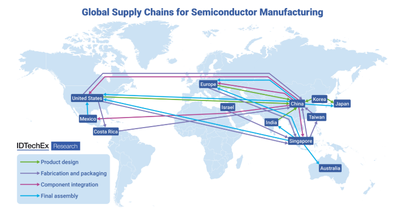
Barriers to sustainable electronics are also assessed, with capital costs and integration of new methods into existing manufacturing techniques complex. A key driver for green electronics will be legislation which is described in detail. This includes new Ecodesign for Sustainable Products Regulation (ESPR) and digital product passports (DPP) legislation coming into effect in Europe. Existing and upcoming legislation in the Asia Pacific (APAC) region is also described. Whilst 90% of PCBs are manufactured in the APAC region, the electronics supply chain flows globally, resulting in localised legislation having a global impact.
For those looking to understand opportunities in sustainable electronics, at all stages of the PCB and IC manufacturing value chain, IDTechEx’s report is a must. Sustainable electronics is currently of critical importance: as demand for electronics continues to grow it is vital for the reduction of environmental impact and compliance with anticipated stricter legislation. In many cases sustainable improvements and operational cost reductions can arrive hand in hand, making implementation desirable on two fronts. The reader will leave equipped with a wide-ranging, in-depth picture of the present and future of sustainable electronics.
Key questions answered in this report
- What are the key policies and legislations to watch out for?
- What are existing low emission technologies that can be implemented?
- What disruptive technologies are on the horizon?
- Which novel manufacturing routes are both sustainable, reliable, and scalable?
- How can additive manufacturing reduce costs and minimise waste?
- Where are the key materials growth opportunities?
- What are key players doing to improve sustainability?
This report from IDTechEx covers the following key aspects:
Technology trends & manufacturer analysis:
- Discussion of emerging materials for printed circuit boards, including flexible, recyclable and biodegradable substrates.
- Comparison of different component attachment materials, including conventional solder, low temperature solder, and electrically conductive adhesives.
- Comparison of wet and dry etching methods with a view to reducing chemical waste and cutting costs.
- Sustainability benchmarking of different materials and manufacturing processes, with key SWOT analysis throughout.
- Insight into what key industry players are doing to enact sustainability measures in their IC fabrication methods, including new materials and processes.
- Water management analysis for IC manufacturing.
- End of life analysis and highlighting of key areas to be improved to reduce the environmental impact and emissions associated with the manufacturing of printed circuit boards and integrated circuits.
- Evaluation of emerging additive manufacturing routes and the companies developing them.
- Assessment of how rising legislation will affect the adoption of new materials and manufacturing processes.
Market forecasts & analysis:
- Market size and 10-year market forecasts segmented by revenue, production volume, materials requirements, energy usage and water usage. Assessment of technological and commercial readiness level for different materials and processes related to the manufacturing of printed circuit boards and integrated circuits.